Liquid crystal device and electronic apparatus

A liquid crystal device and liquid crystal layer technology, applied in folders, optics, printing, etc., can solve the problems of reduced pixel aperture ratio, large gap area, unable to display images, etc., and achieve the effect of excellent viewing angle characteristics and high pixel aperture ratio.

Inactive Publication Date: 2006-09-06
JAPAN DISPLAY INC
View PDF0 Cites 4 Cited by
  • Summary
  • Abstract
  • Description
  • Claims
  • Application Information

AI Technical Summary

Problems solved by technology

[0007] However, as in the technology described in Non-Patent Document 2, when a plurality of slits are formed on the entire outer periphery of the sub-pixel, there is a problem that the pixel aperture ratio is reduced because the area of ​​the slit that is not directly used for display is large. (The ratio of the part directly used for display to the whole pixel) is significantly reduced, and bright images cannot be displayed

Method used


Image

  • Liquid crystal device and electronic apparatus
  • Liquid crystal device and electronic apparatus
  • Liquid crystal device and electronic apparatus

Examples


Embodiment approach 1

[0041] (the whole frame)

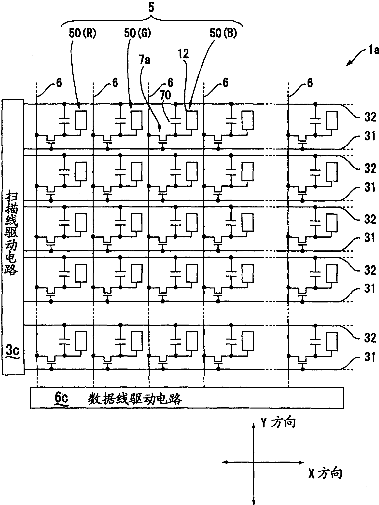
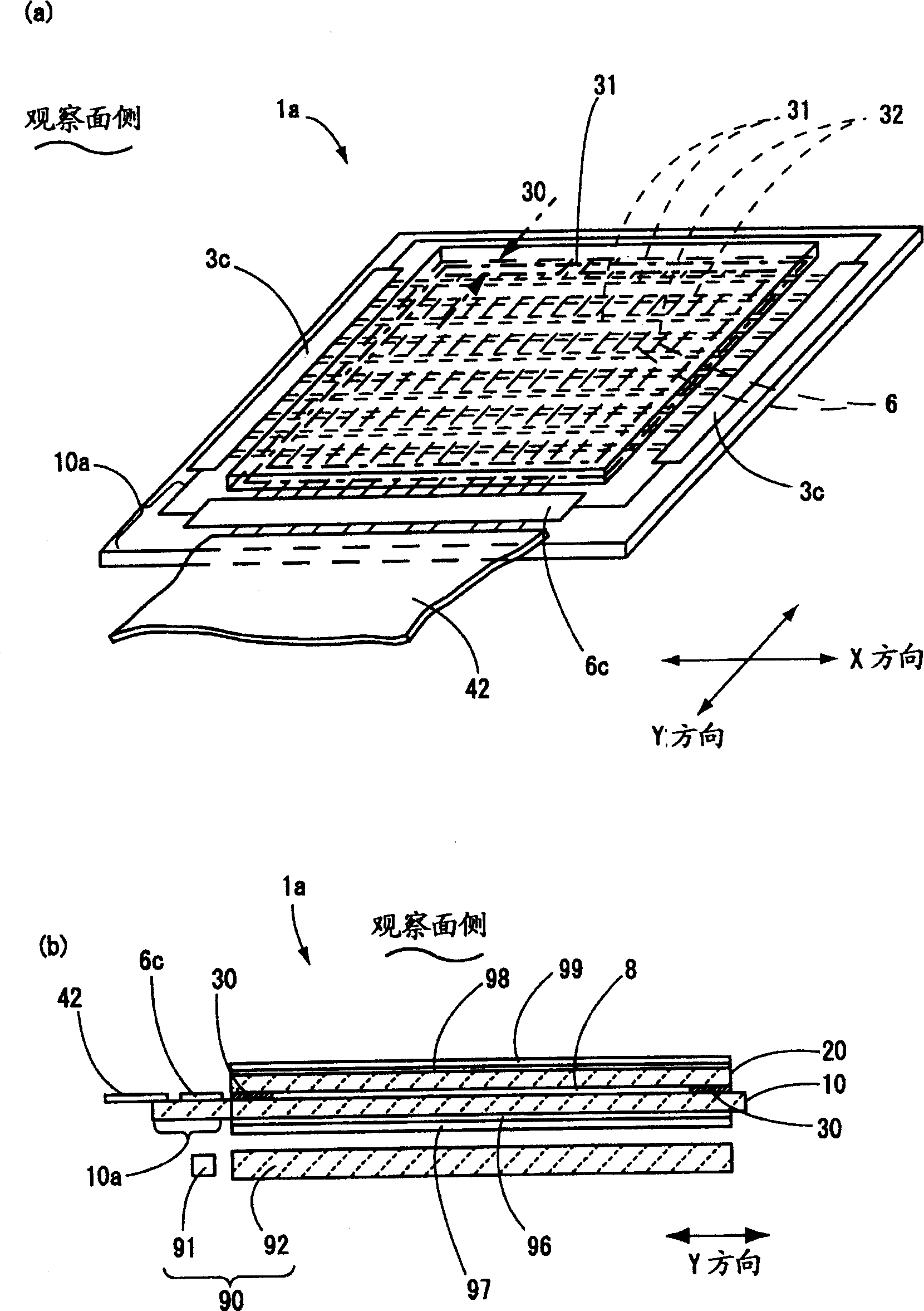
[0042] figure 1 It is a block diagram showing the electrical configuration of the liquid crystal device according to Embodiment 1 of the present invention. figure 2 (a) and (b) are schematic perspective views of the liquid crystal device according to Embodiment 1 of the present invention seen from obliquely above (counter substrate) side, and explanatory diagrams schematically showing a cross-section when the liquid crystal device is cut in the Y direction . In addition, since the liquid crystal device of this form is used for color display, each pixel corresponds to red (R), green (G), and blue (B). (R), (G), (B) to represent.

[0043] figure 1 The shown liquid crystal device 1a is a transmissive active matrix liquid crystal device using TFT (Thin Film Transistor, thin film transistor) as a pixel switching element, and a plurality of scanning lines 31 as signals are formed in the X direction (row direction), A plurality of data lines 6 are f...

Embodiment approach 2

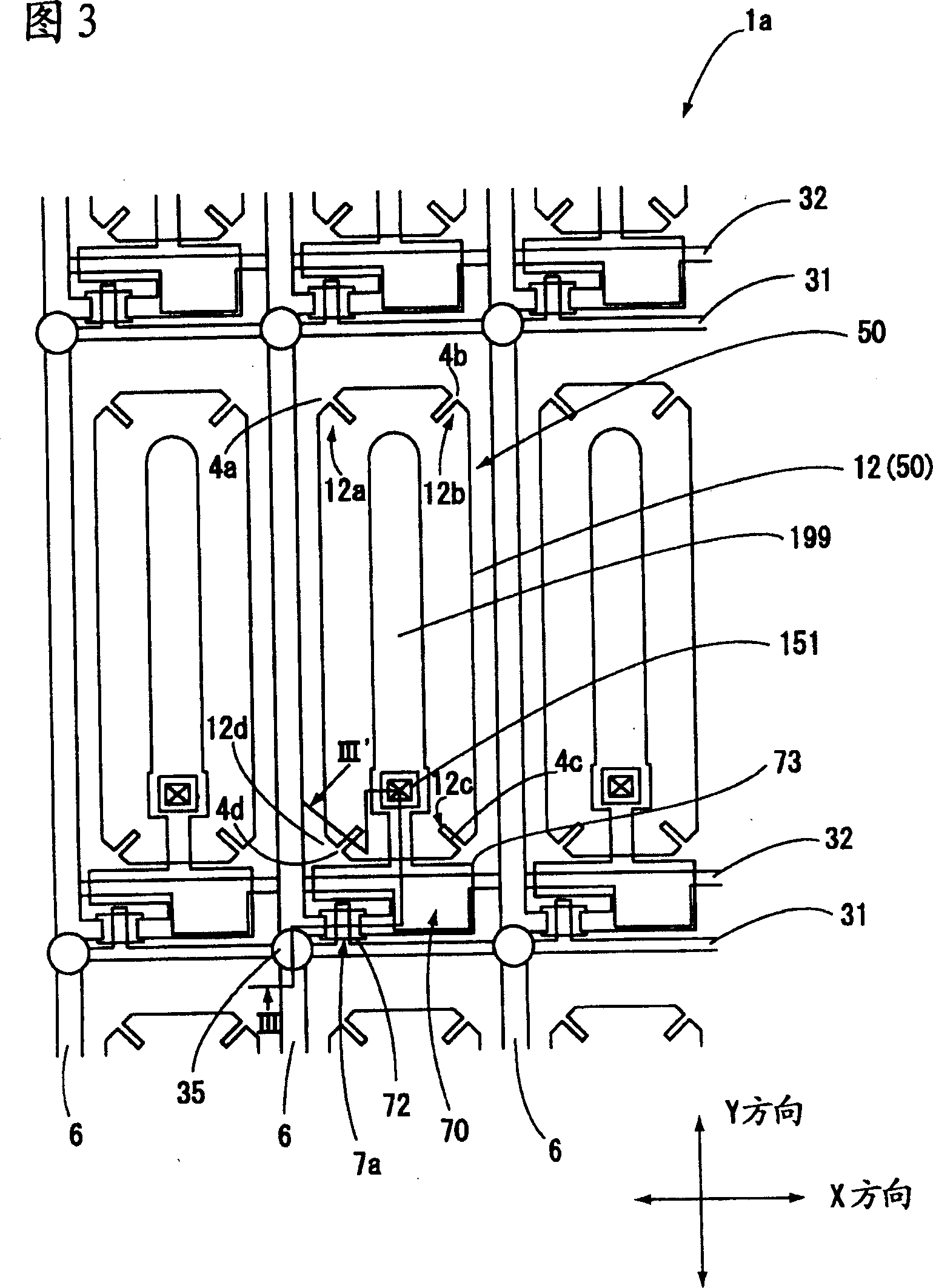
[0060] 5 is a plan view schematically showing a pixel structure in the range of one dot of the liquid crystal device according to Embodiment 2 of the present invention. 6 is an enlarged cross-sectional view showing one of a plurality of pixels formed in the liquid crystal device according to Embodiment 2 of the present invention, and corresponds to the V-V' cross-sectional view in FIG. 5 . Figure 7 (a) and (b) are explanatory diagrams showing equipotential lines when a slit is formed on a sub-pixel electrode in the liquid crystal device according to Embodiment 2 of the present invention. In addition, since the basic structure of the liquid crystal device of this embodiment is the same as that of Embodiment 1, the same parts are shown with the same symbols and their descriptions are omitted.

[0061] The liquid crystal device 1a shown in FIGS. 5 and 6 is also the same as Embodiment 1, and is a transmissive active-matrix liquid crystal device using TFTs as pixel switching eleme...

Embodiment approach 3

[0075]8 is a plan view schematically showing a pixel structure in a range of one dot of a liquid crystal device according to Embodiment 3 of the present invention. 9 is an enlarged cross-sectional view showing one of the plurality of pixels formed in the liquid crystal device according to Embodiment 3 of the present invention, and corresponds to the VIII-VIII' cross-sectional view in FIG. 8 . In addition, since the basic structure of the liquid crystal device of this embodiment is the same as that of Embodiment 1, the same reference numerals are attached to the same parts, and their descriptions are omitted.

[0076] The liquid crystal device 1a shown in FIGS. 8 and 9 is different from Embodiment 1 in that it is a transflective active matrix liquid crystal device. Reflective layer 16 made of aluminum alloy or silver alloy is formed on the following region among the layers of electrode 12 . In addition, the interlayer insulating film 15 is formed using a photosensitive resin a...


PUM


Abstract

A liquid crystal device includes a first substrate that has an inner surface on which a pixel electrode is formed; a second substrate that has an inner surface on which a counter electrode constituting a pixel is formed opposite to the pixel electrode; and a liquid crystal layer that is held between the first substrate and the second substrate and has negative dielectric anisotropy. In addition, an alignment control unit for controlling the alignment of the liquid crystal molecules is formed in an area including the center of the pixel electrode on either the first substrate or the second substrate; and the pixel electrode has an approximately polygonal shape, and slits extending from an outer periphery toward the center are formed at corner portions of the pixel electrode.

Description

technical field [0001] The present invention relates to a liquid crystal device and electronic equipment provided with the liquid crystal device. The liquid crystal device uses a liquid crystal having a negative dielectric constant anisotropy. Background technique [0002] In general, an active matrix liquid crystal device has: a first substrate, on which a pixel electrode is formed on the inner surface; a second substrate, on which an opposite electrode that is opposite to the pixel electrode to form a pixel is formed on the inner surface; and a liquid crystal layer, held on the second substrate between the 1st substrate and the 2nd substrate. In such liquid crystal devices, VA (Vertical Alignment, Vertical Alignment) that vertically aligns the substrate with a liquid crystal having a negative dielectric anisotropy and tilts the liquid crystal by applying a voltage has been proposed as a technique for improving its viewing angle characteristics. Scheme of the mode (for exa...

Claims


Application Information

Patent Timeline
Patent Type & Authority Applications(China)
IPC IPC(8): G02F1/133G02F1/1337G02F1/1343
CPCG02F1/133707G02F1/134309G02F1/1393B42F13/14
Inventor 仓泽隼人
Owner JAPAN DISPLAY INC
Why Eureka
Try Eureka