Method for detecting semiconductor micro device bonding strength

A bonding strength and micro-device technology, which is applied in semiconductor/solid-state device testing/measurement, etc., can solve the problems of device electrodes or circuits, adding more solder, and inconvenient bonding, etc., to achieve stable process, simple process, and bond The effect of low combined temperature

Inactive Publication Date: 2006-09-06
PEKING UNIV
View PDF0 Cites 2 Cited by
  • Summary
  • Abstract
  • Description
  • Claims
  • Application Information

AI Technical Summary

Problems solved by technology

Among them, Si-Si bonding has the highest precision, but the temperature used is also the highest, which is about 1000°C, which brings inconvenience to the bonding; Si-Glass bonding has a lower temperature, about 400°C, but the precision is lower. Moreover, a high voltage must be applied, which will affect the electrodes or circuits in the device; Flip Chip welding also has low precision and requires more solder

Method used


Image

  • Method for detecting semiconductor micro device bonding strength
  • Method for detecting semiconductor micro device bonding strength
  • Method for detecting semiconductor micro device bonding strength

Examples


Embodiment 1

[0044] Example 1. Three-layer bonding of piezoresistive accelerometer

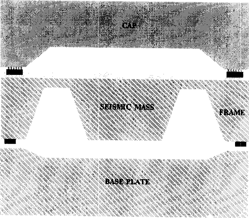
[0045] The cross-sectional structure of the piezoresistive accelerometer is as follows: figure 2 shown. Its three-layer structure needs to be assembled together by bonding. A 4-inch 525 μm thick n-(100) silicon structural wafer is used, and the middle layer is a double-sided polished structural wafer. Firstly, silicon wafers are subjected to a conventional acid boiling process, that is, silicon wafers are soaked in a mixed solution of sulfuric acid and hydrogen peroxide (H 2 SO 4 :H 2 o 2 =4:1) and boiled (about 120°C) for 10 minutes to remove pollutants and hydrocarbons on the surface of the silicon wafer. One surface of the structural sheet is sputtered with a Cr layer of 200-500 Å and an Au layer of about 3000 Å, and its structure is a silicon matrix-SiO 2 / Cr / Au, while the other side is pure silicon base (rinsed with BHF solution before bonding to remove the natural oxide layer) and matrix-SiO ...

Embodiment 2

[0053] Embodiment 2: testing bonding strength by pressing arm method

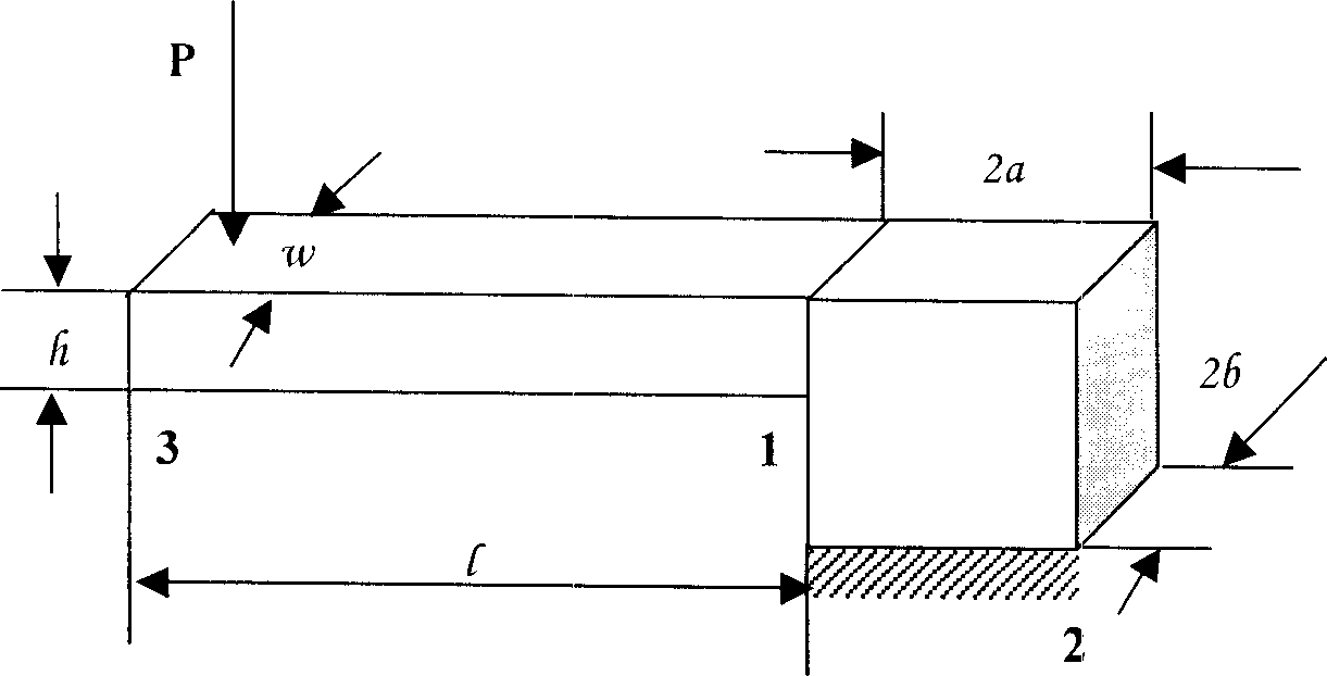
[0054]Compression arm method to test the bonding strength, such as figure 1 Shown:

[0055] According to a series of design calculations, the length range of the pressing arm can be obtained:

[0056] 4 a 3 [ σ 2 ] - 2 Pa 3 P ≤ l ≤ ah 2 [ σ 1 ] 3 P - - - ( I )

[0057] Substituting the relevant parameters, it can be approximat...


PUM


Abstract

The present invention discloses a method for detecting semiconductor micro - device bond strength. Said method is according to formula (II) designing a group of similar press arm pattern: 8 alpha / 3 <=l <= 50000 / alpha (II), measuring bonding surface crack in one length L, then calculating or comparing bond strength. Said invented method can conveniently detecting bond strength of semiconductor micro - device.

Description

technical field [0001] The present invention is a divisional application filed on May 6, 2003, the application number is 03130642.x, and the title of the invention is "a bonding method for semiconductor micro-devices and its bonding strength detection method". The invention relates to a detection method for bonding strength of semiconductor micro devices. Background technique [0002] Bonding and packaging are important components in the manufacturing process of semiconductor microdevices (including various functional chips, sensors and other microelectronic devices). Studies have shown that its cost often accounts for 70% or more of the entire device or chip. At present, the bonding technology in semiconductor micro-devices mainly includes Si-Si bonding, Si-Glass bonding and flip-chip welding FlipChip, etc. Among them, Si-Si bonding has the highest precision, but the temperature used is also the highest, around 1000°C, which brings inconvenience to the bonding; Si-Glass b...

Claims


Application Information

Patent Timeline
Patent Type & Authority Applications(China)
IPC IPC(8): H01L21/66
Inventor 王翔张大成李婷王玮王颖
Owner PEKING UNIV
Why Eureka
Try Eureka