CMOS image transducer

An image sensor, pixel array technology, applied in image communication, electric solid state devices, semiconductor devices, etc., can solve the problems of narrow dynamic range, excess signal-to-noise ratio, high power consumption, etc., achieve wide dynamic range, eliminate interference, low The effect of power consumption

Inactive Publication Date: 2006-09-20
BEIJING SUPERPIX MICRO TECHNOLOGY CO LTD
View PDF0 Cites 22 Cited by
  • Summary
  • Abstract
  • Description
  • Claims
  • Application Information

AI Technical Summary

Problems solved by technology

[0013] It can be seen from this that the existing CMOS image sensor is due to the inherent defect of the linear quantization method, that is, the signal-to-noise ratio is sufficient when the signal is large, and the signal-to-noise ratio is insufficient when the signal is small, so that th

Method used


Image

  • CMOS image transducer
  • CMOS image transducer
  • CMOS image transducer

Examples


Embodiment Construction

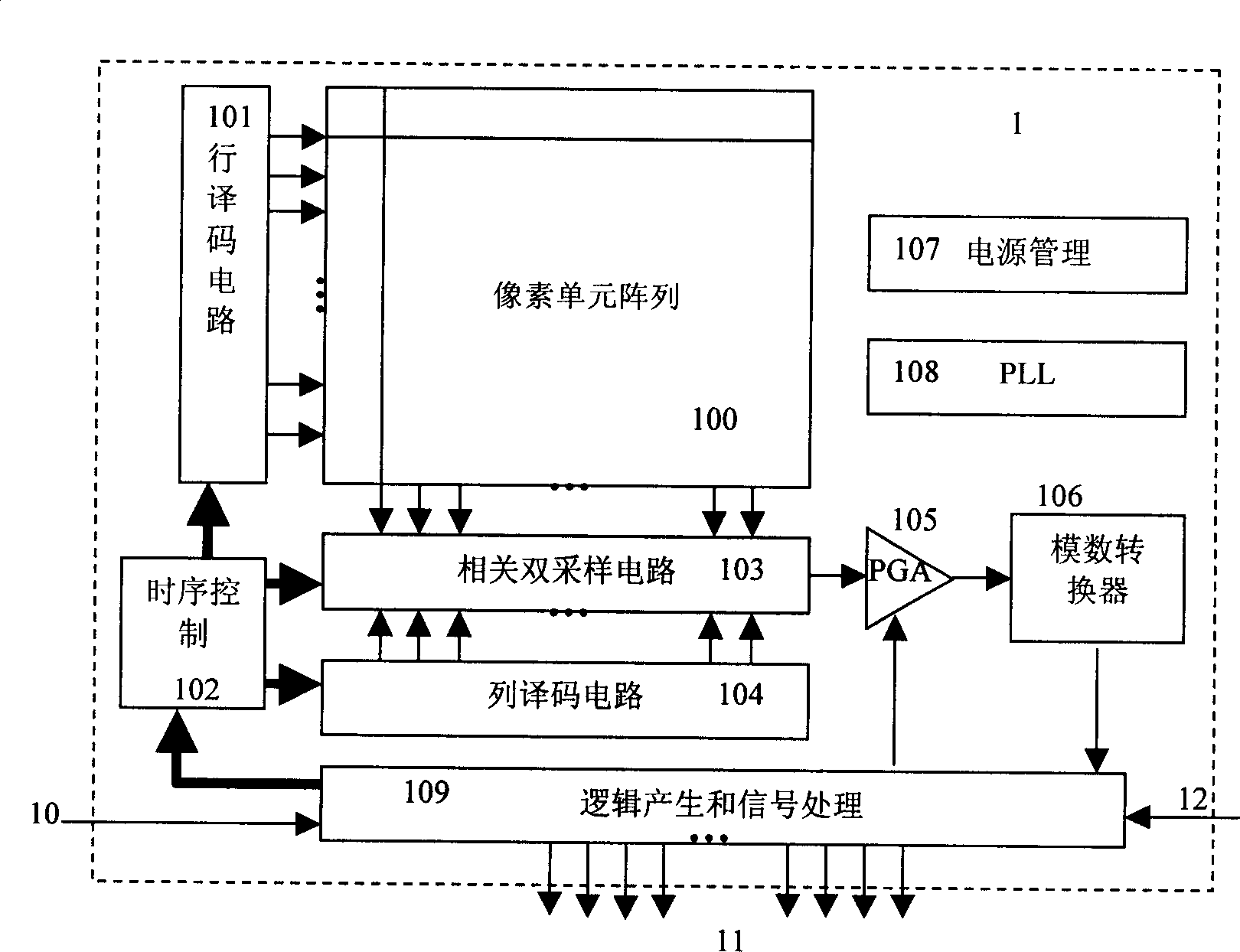
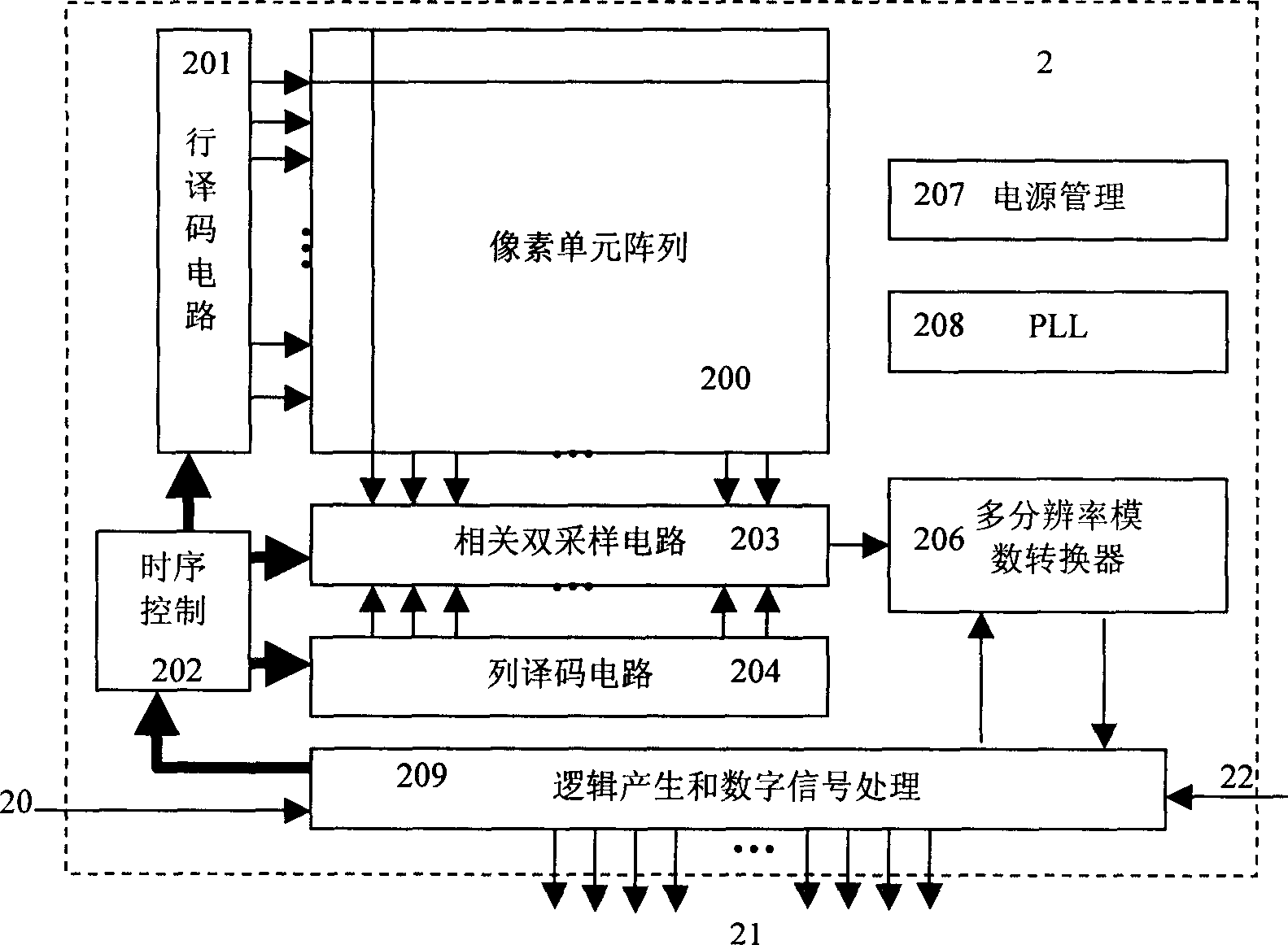
[0041] The specific embodiment of the novel CMOS image sensor of the present invention is as follows figure 2As shown, the pixel unit array 200 is composed of m rows by n columns of pixel unit circuits, and the pixel unit circuit specifically adopts a logarithmic response structure. Therefore, the optical signal is converted into an electrical signal as a multi-resolution change, which can expand the dynamic range of the pixel response. The row address of the pixel unit array 200 is generated by the row decoding circuit 201, and the rows of pixels are sequentially scanned from top to bottom or bottom to top. The column address of the pixel unit array 200 is generated by the column decoding circuit 204, and the row pixels are sequentially scanned from left to right or from right to left. The row decoding circuit 201 and the column decoding circuit 204 can also generate and read out image signals of any unit pixel or any window in the pixel unit array 200 at random. When a ce...


PUM


Abstract

The CMOS image sensor comprises a pixel matrix, a row decoder correspondingly connected to the rows in the pixel matrix, and a column decode correspondingly connected to the columns in the pixel matrix through a correlated double sampling circuit. The pixel matrix is composed of a group of pixel element circuits, which are logarithm type response pixel element circuits. The logarithm type response pixel element circuits includes a transistor connected to power supply and working at sub-threshold area for use in implementing the logarithm type response of the pixel element circuit. In the invention, an A/D conversion by a multi resolution quantization A/D converter can be adopted to make A/D conversion, amplify the signal at low light level and compress the signal at high light level in order to get a dynamical range over 80 db.

Description

technical field [0001] The invention relates to integrated circuit design in the technical field of electronic circuits, in particular to a CMOS image sensor. Background technique [0002] With the development of CMOS process technology and circuit design technology, the performance of CMOS image sensor has been greatly improved, which is reflected in: the readout noise is effectively reduced by adopting a new process and correlated double sampling circuit, and the filling is improved by using microlens technology. coefficient, the use of buried photodiodes and small-size CMOS technology effectively reduces the dark current of the photodetector. Therefore, CMOS image sensors are developing towards high resolution, low noise, high integration and wide dynamic range. [0003] However, current CMOS image sensors still have defects such as low signal-to-noise ratio, low quantum efficiency, and narrow dynamic range. [0004] The CMOS image sensor in the prior art mainly include...

Claims


Application Information

Patent Timeline
IPC IPC(8): H04N3/15H01L27/14H04N5/374H04N5/378
Inventor 金湘亮
Owner BEIJING SUPERPIX MICRO TECHNOLOGY CO LTD
Why Eureka
Try Eureka