Check patentability & draft patents in minutes with Patsnap Eureka AI!

Polarized non-sensitive array waveguide grating

An arrayed waveguide grating and arrayed waveguide technology, applied in the field of arrayed waveguide gratings, can solve problems such as device performance degradation and complex structure, and achieve the effects of low cost, simple working principle, and simple production

Inactive Publication Date: 2006-09-27
杭州兰特普光电技术有限公司
View PDF0 Cites 9 Cited by
  • Summary
  • Abstract
  • Description
  • Claims
  • Application Information

AI Technical Summary

Problems solved by technology

[0015] The purpose of the present invention is to address the deficiencies in the prior art and propose a polarization-insensitive arrayed waveguide grating, which solves the problems of poor device performance and complex structure caused by the traditional arrayed waveguide grating polarization compensation method

Method used


Image

  • Polarized non-sensitive array waveguide grating
  • Polarized non-sensitive array waveguide grating
  • Polarized non-sensitive array waveguide grating

Examples


Embodiment 1

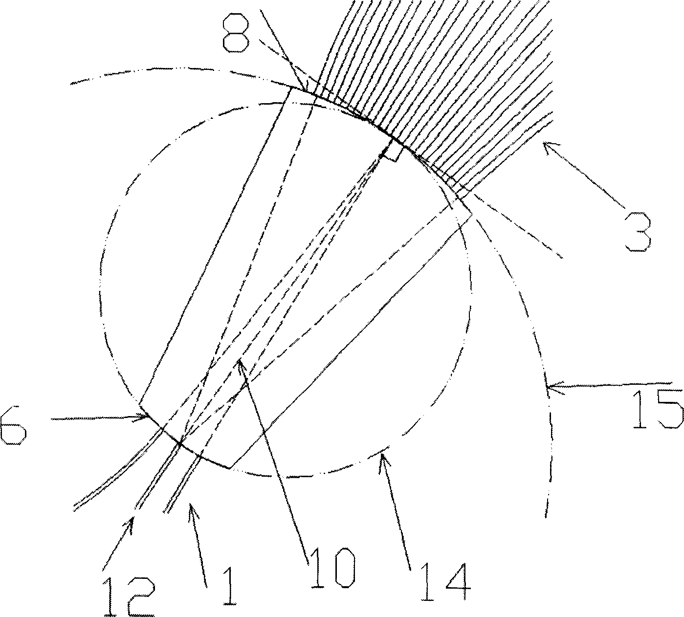
[0052] Δλ s = 0.6nm, Δλ a =-0.2nm; Δn s =5.6232*10 -4 , Δn a =-1.8708*10 -4

[0053] Solve to get α=28.695°, ΔL s = 4.802 μm, ΔL = 28.865 μm.

[0054] The device size is 36.667mm×17.969mm.

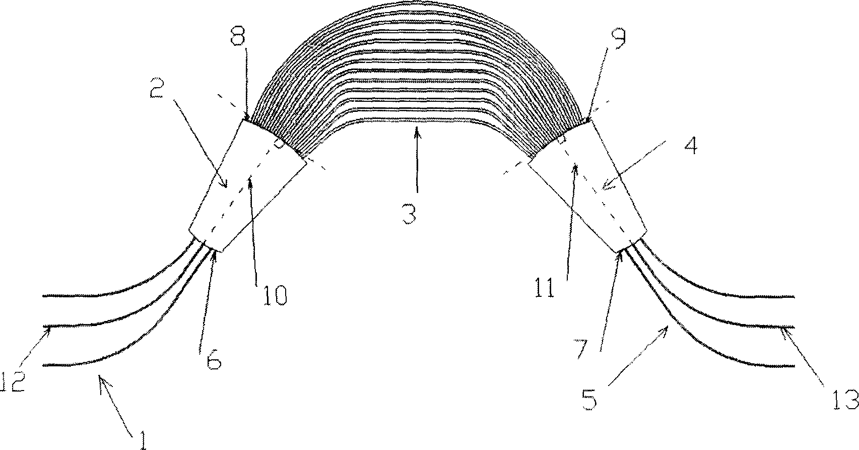
[0055] The resulting polarization-insensitive arrayed waveguide grating layout is as follows Figure 5 shown. For the sake of clarity, not all arrayed waveguides are drawn in the figure, but some arrayed waveguides are drawn for illustration.

Embodiment 2

[0057] Δλ s = 0.6nm, Δλ a = 0.2nm; Δn s =5.6232*10 -4 , Δn a =1.8708*10 -4

[0058] Solve to get α=-47.620°, ΔL s =-9.603 μm, ΔL=57.729 μm.

[0059] The device size is 36.589mm×16.280mm.

[0060] The layout of the resulting polarization-insensitive AWG is shown in Figure 7. For the sake of clarity, not all arrayed waveguides are drawn in the figure, but some arrayed waveguides are drawn for illustration.


PUM


Abstract

This invention relates to a polarized non-sensitive array waveguide grating. Unlike to traditional product, the optical path difference of This grating origins both from the array waveguide zone and the plane plate waveguide zone; it compensates the array zone with the birefringence property of plane plate waveguide zone, and sets the included angle between the tangent curve of adjacent curve center of two zones and the plant plate zone OA within 0 and 180Deg but not equal to 90Deg. This invention compensates the polarization dispersion without extra device, and has wide application as low cost.

Description

technical field [0001] The invention relates to the technical field of wavelength division multiplexing, in particular to a polarization-insensitive arrayed waveguide grating. Background technique [0002] After entering the 21st century, the information industry has developed rapidly and has become an important part of the national economic structure. Its development scale and level have become important indicators to measure the comprehensive national strength. The optical communication industry is one of its main components, leading the development direction of the information communication industry. As one of the core components in the wavelength division multiplexing optical communication system, the integrated arrayed waveguide grating will be more and more widely used. [0003] In 1988, Smit proposed a new type of integrated optical waveguide wavelength division multiplexer / demultiplexer - Arrayed Waveguide Grating (AWG). After years of development, the performance ...

Claims


Application Information

Patent Timeline
IPC IPC(8): G02B6/124H04J14/02
Inventor 何建军郎婷婷何赛灵
Owner 杭州兰特普光电技术有限公司
Features
  • R&D
  • Intellectual Property
  • Life Sciences
  • Materials
  • Tech Scout
  • Unparalleled Data Quality
  • Higher Quality Content
  • 60% Fewer Hallucinations
Learn More