Electric non-polarized composite gallium nitride base substrate and production method
A GaN-based, non-polarized technology, applied in circuits, electrical components, semiconductor devices, etc., can solve the problems of current congestion, easy breakdown of devices, uneven current distribution, etc., and achieve the effect of high heat conduction efficiency
- Summary
- Abstract
- Description
- Claims
- Application Information
AI Technical Summary
Problems solved by technology
Method used
Image
Examples
example
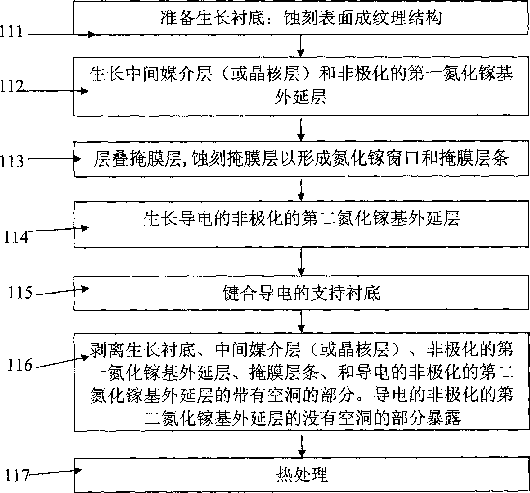
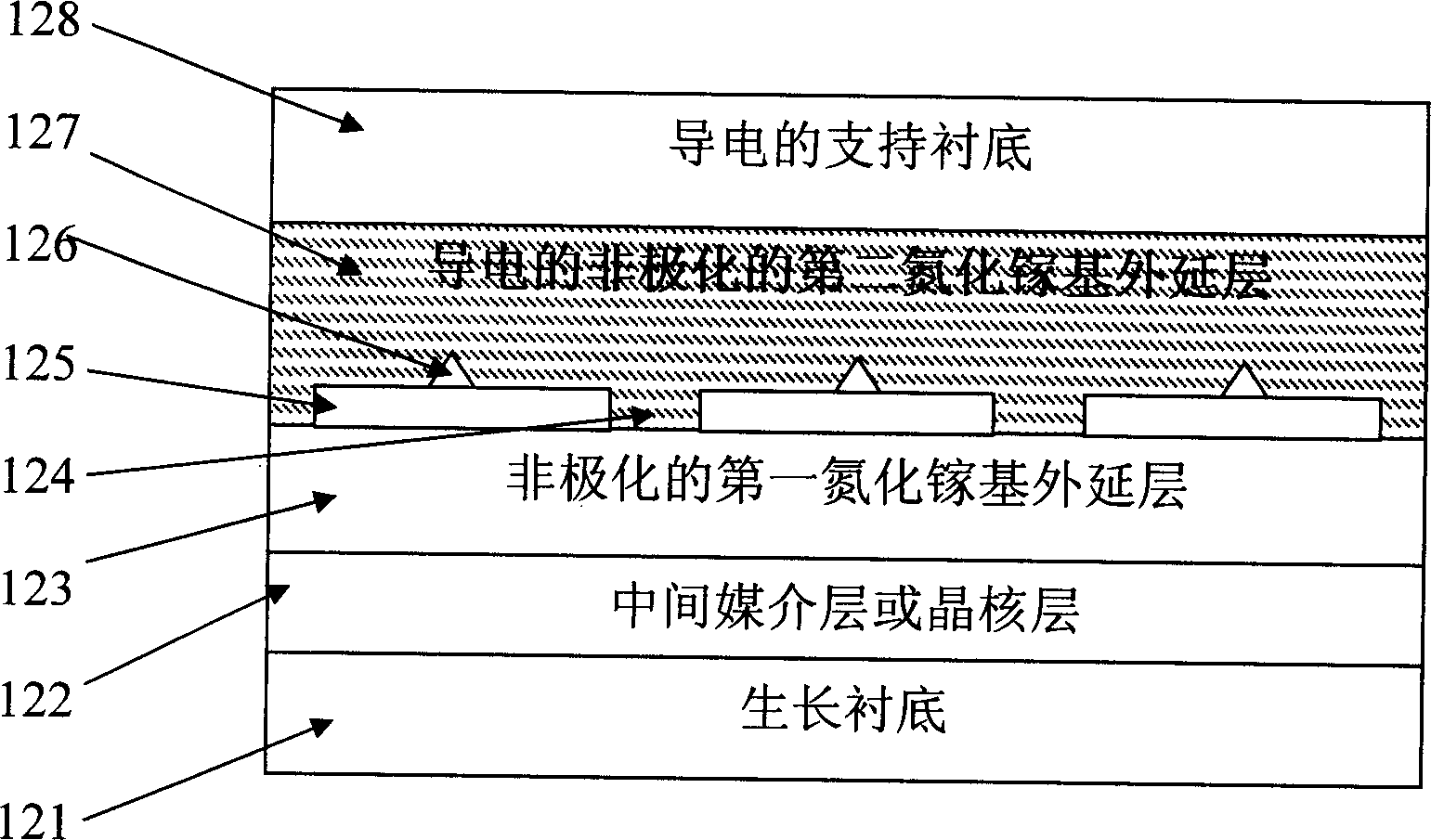
[0047] The first specific implementation example of the process flow step 112: using MOCVD, grow a layer of gallium nitride substrate with a thickness between 1 nm and 90 nm on the r-plane sapphire growth substrate (at a temperature of 400-900 ° C). Nucleation layer. The material of the crystal nucleus layer includes, but is not limited to, gallium nitride. An a-plane non-polarized first GaN-based epitaxial layer is grown on the crystal nucleus layer. A specific implementation example of growing a non-polarized a-plane first gallium nitride-based epitaxial layer: growing a non-polarized a-plane at a temperature above about 1000° C. and at a pressure less than 1 atmosphere, with an appropriate V / III ratio The thickness of the first GaN-based epitaxial layer is 1-5 microns.
[0048] A second specific implementation example of process flow step 112: using MBE, grow an aluminum nitride buffer layer on an m-plane 6H-silicon carbide growth substrate, and then grow an m-plane first...
PUM
 Abstract
Description
Claims
Application Information
 - R&D
- Intellectual Property
- Life Sciences
- Materials
- Tech Scout
- Unparalleled Data Quality
- Higher Quality Content
- 60% Fewer Hallucinations
Browse by: Latest US Patents, China's latest patents, Technical Efficacy Thesaurus, Application Domain, Technology Topic, Popular Technical Reports.
© 2025 PatSnap. All rights reserved.Legal|Privacy policy|Modern Slavery Act Transparency Statement|Sitemap|About US| Contact US: help@patsnap.com


