Production of semiconductor component and method for adjusting component channel area lattice distance

A manufacturing method and a technology for adjusting components, which are applied in semiconductor/solid-state device manufacturing, electrical components, circuits, etc., to achieve the effects of improving charge mobility, improving component performance, and increasing process costs

Inactive Publication Date: 2006-11-01
UNITED MICROELECTRONICS CORP
View PDF0 Cites 4 Cited by
  • Summary
  • Abstract
  • Description
  • Claims
  • Application Information

AI Technical Summary

Problems solved by technology

However, on the other hand, as the device size becomes smaller and smaller, the effect of the lattice distance in the channel region 128 on the charge mobility becomes more and more significant, and this will become a key factor affecting device performance

Method used


Image

  • Production of semiconductor component and method for adjusting component channel area lattice distance
  • Production of semiconductor component and method for adjusting component channel area lattice distance
  • Production of semiconductor component and method for adjusting component channel area lattice distance

Examples


Embodiment Construction

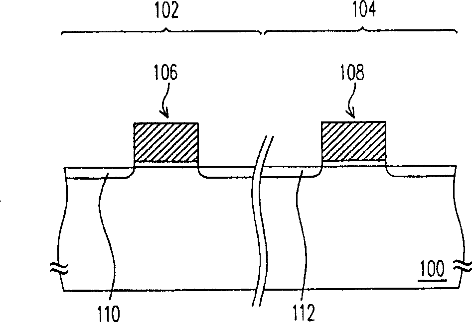
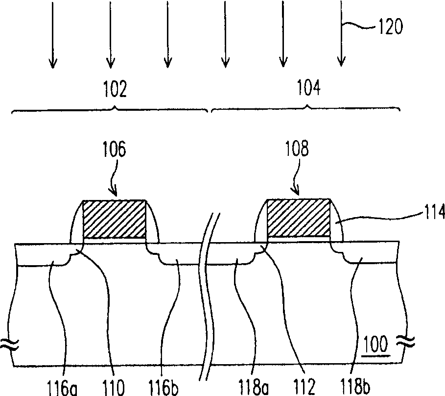
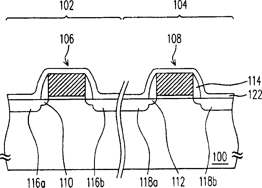
[0041] Figure 2A to Figure 2F is a schematic cross-sectional view illustrating a manufacturing process of a semiconductor device according to a preferred embodiment of the present invention. Please refer to Figure 2A , providing a substrate 200 , for example, the substrate 200 has a main device area 202 and a peripheral circuit area 204 . Then, gate structures 206 and 208 are formed on the substrate 200 in the main device area 202 and the peripheral circuit area 204 respectively. Wherein, the gate structure 206 is, for example, a part of a memory element or an ESD protection circuit, which is composed of a gate dielectric layer 206a located on the lower layer and a gate layer 206b located on the upper layer. In addition, the gate structure 208 is, for example, a part of a logic device, which is composed of a gate dielectric layer 208a located on the lower layer and a gate layer 208b located on the upper layer. In addition, the material of the gate dielectric layers 206 a ...


PUM

PropertyMeasurementUnit
thicknessaaaaaaaaaa

Abstract

The method comprises: forming several grid structures on the substrate; forming a corresponding source region and a drain region on the portion of substrate aside each grid structure; forming a self-alignment metal silicides barrier layer on the substrate to overlap the grid structure and the surface of exposed substrate; making annealing practice, and when the annealing practice is made, the self-alignment metal silicides barrier layer will generate a tensile stress to make the substrate under the grid structure suffered the tensile stress; removing a portion of self-alignment metal silicides barrier layer to expose a portion of grid structure and a portion of substrate surface; making the self-alignment metal silicides process.

Description

technical field [0001] The invention relates to a semiconductor process, in particular to a manufacturing method of a semiconductor element and a method for adjusting the lattice distance of the channel region of the element. Background technique [0002] Early Metal-Oxide Semiconductor (MOS) devices are composed of a metal gate layer, a silicon oxide gate dielectric layer and a semiconductor silicon substrate. However, because most metals have poor adhesion to silicon oxide, most current gate layers are made of polysilicon. However, the use of polysilicon has led to other problems, such as the degradation of device performance due to the high resistance of polysilicon. Therefore, the currently adopted method is to perform a silicide process after the device is formed to form a layer of metal silicide on the gate layer and the source / drain region, thereby reducing the resistance of the device. [0003] On the other hand, a wafer can usually be divided into a main element a...

Claims


Application Information

Patent Timeline
Patent Type & Authority Applications(China)
IPC IPC(8): H01L21/336H01L21/8234
Inventor 刘毅成黄正同萧维沧廖宽仰
Owner UNITED MICROELECTRONICS CORP
Why Eureka
Try Eureka