Semiconductor device and manufacturing method thereof
A semiconductor and device technology, applied in the field of semiconductor devices and their manufacturing, can solve problems such as high resistance of impurity diffusion layers or increased joint leakage, and achieve the effect of inhibiting abnormal growth and condensation
- Summary
- Abstract
- Description
- Claims
- Application Information
AI Technical Summary
Problems solved by technology
Method used
Image

Examples
no. 1 example
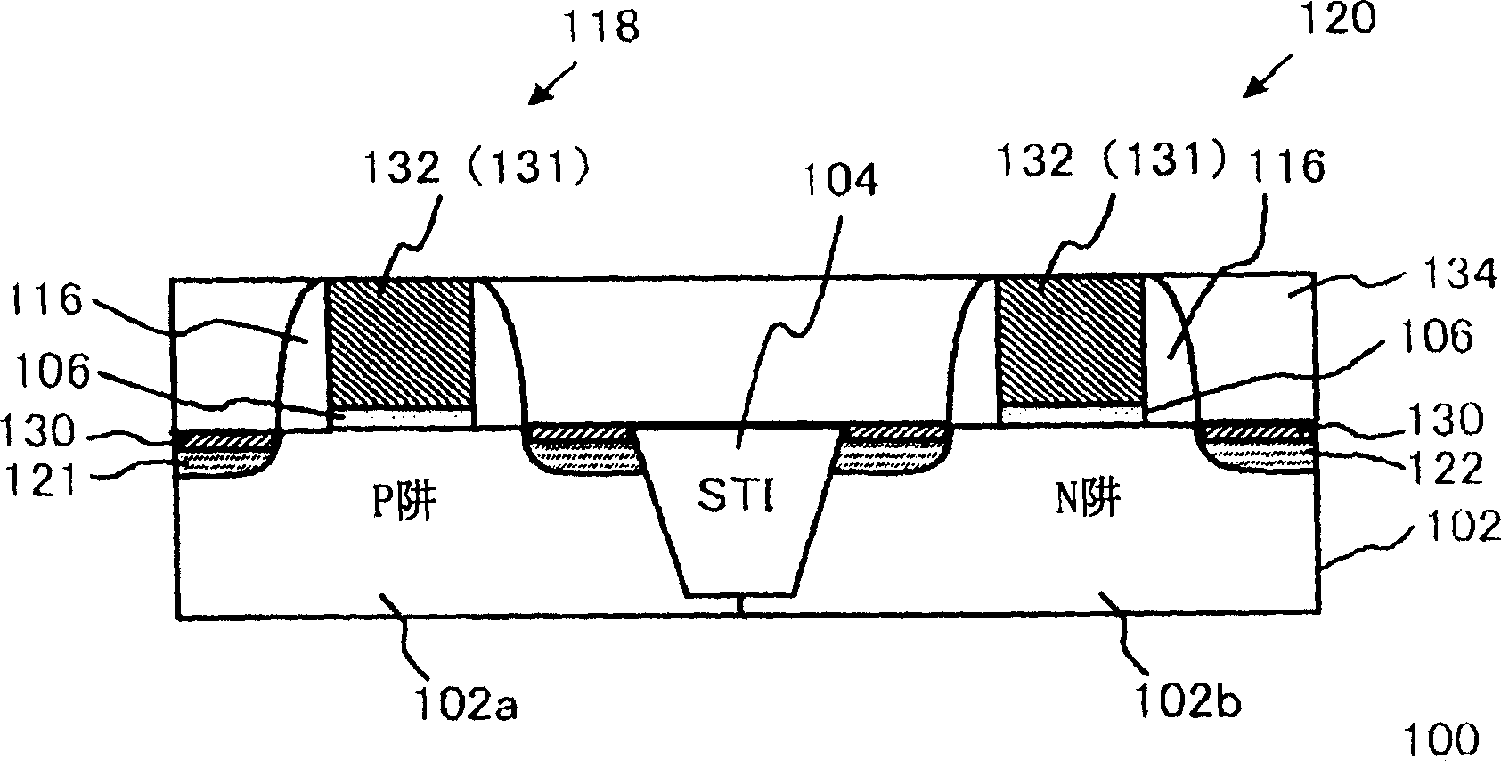
[0043] figure 1 is a cross-sectional view showing the configuration of the semiconductor device of the present embodiment. In the present embodiment, the semiconductor device 100 is a CMOS (Complementary Metal Oxide Semiconductor) device including an N-type MOSFET 118 and a P-type MOSFET 120 . In addition, this CMOS device constitutes the internal circuit of the LSI.
[0044] The semiconductor device 100 includes: a silicon substrate 102, a P-well 102a of a P-type conductor and an N-well 102b of an N-type conductor; and an element isolation region 104 for isolating the P-well 102a and the N-well 102b. N-type MOSFET 118 and P-type MOSFET 120 are formed at P-well 102a and N-well 102b, respectively. Interlayer insulating film 134 covering the sides of N-type MOSFET 118 and P-type MOSFET 120 is formed on silicon substrate 102 .
[0045] A pair of impurity diffusion layers 121 are provided at the P well 102a, and a channel region is formed between these impurity diffusion layers...
no. 2 example
[0082] In the present embodiment, a part of the process for manufacturing the semiconductor device 100 is different from the first embodiment. The following is a reference Figure 5A to 5C are descriptions of the method of manufacturing the semiconductor device of the present embodiment. Figure 5A to 5C are process sectional views showing a part of the process of manufacturing the semiconductor device 100 of the present embodiment.
[0083] Likewise, in this embodiment, use the same reference as in the first embodiment Figures 2A to 2C , 3A and 3B described the same process formed with Figure 3B The structure shown is the same structure. The protective film 140 is selectively removed by, for example, dry etching, and the polysilicon film 114 is exposed ( Figure 5A ).
[0084] Next, a second metal layer 144 (having a film thickness of, for example, 5 nm to 10 nm) is formed on the entire surface on the silicon substrate 102 ( Figure 5B ). Thereafter, a second heat tr...
no. 3 example
[0088] In the present embodiment, a part of the process for manufacturing the semiconductor device 100 is different from the first embodiment. The following is a reference Figures 6A to 6C , 7A, 7B, and 8A to 8C are descriptions of the method of manufacturing a semiconductor device of the present embodiment. Figures 6A to 6C , 7A, 7B, and 8A to 8C are process cross-sectional views showing a part of the process of manufacturing the semiconductor device 100 of the present embodiment.
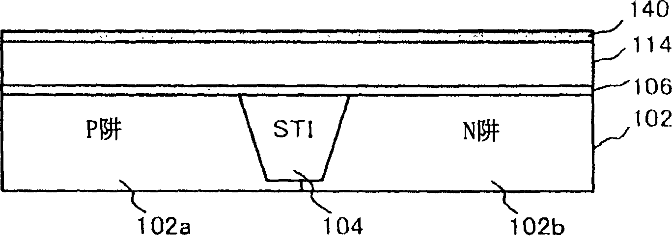
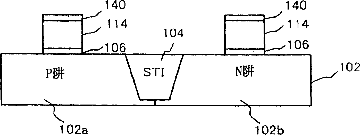
[0089] First, as described in the first embodiment, the element isolation region 104, the P well 102a, and the N well 102b are formed on the silicon substrate 102, and the gate insulating film 106 and the polysilicon film 114 are formed on the silicon substrate 102 ( Figure 6A ). This embodiment differs from the first embodiment in that protective film 140 is not formed on polysilicon film 114 .
[0090] Next, selective etching is performed to form a gate shape in such a manner that a predet...
PUM
 Abstract
Description
Claims
Application Information
 - R&D
- Intellectual Property
- Life Sciences
- Materials
- Tech Scout
- Unparalleled Data Quality
- Higher Quality Content
- 60% Fewer Hallucinations
Browse by: Latest US Patents, China's latest patents, Technical Efficacy Thesaurus, Application Domain, Technology Topic, Popular Technical Reports.
© 2025 PatSnap. All rights reserved.Legal|Privacy policy|Modern Slavery Act Transparency Statement|Sitemap|About US| Contact US: help@patsnap.com