

Method for making T-type grating of transistor circuit with high electron mobility
A technology with high electron mobility and manufacturing method, which is applied in the field of ultra-high-speed microelectronic devices, can solve the problems of increasing process steps, and achieve the effects of simplifying process steps, strong controllability, and easy peeling
Inactive Publication Date: 2006-11-22
SEMICON MFG INT (SHANGHAI) CORP +1
View PDF0 Cites 9 Cited by
- Summary
- Abstract
- Description
- Claims
- Application Information
AI Technical Summary
Problems solved by technology
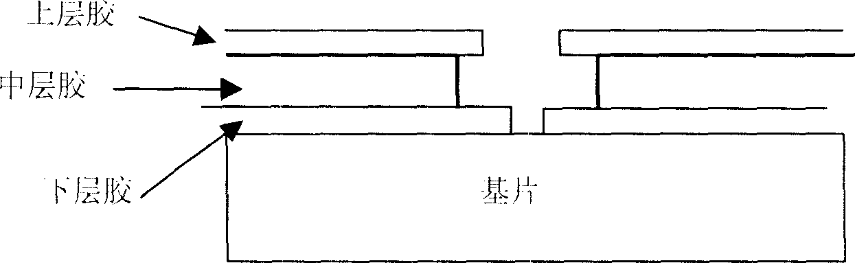
Deposit SiO2 or Si3N4 on the substrate and then apply three layers of glue ZEP / PMGI / ZEP electron beam exposure and develop step by step. Dielectric film deposition is required, and dielectric etching is required after development, which increases the process steps.
Method used
View moreImage
Smart ImageViewing Examples

Examples
Embodiment
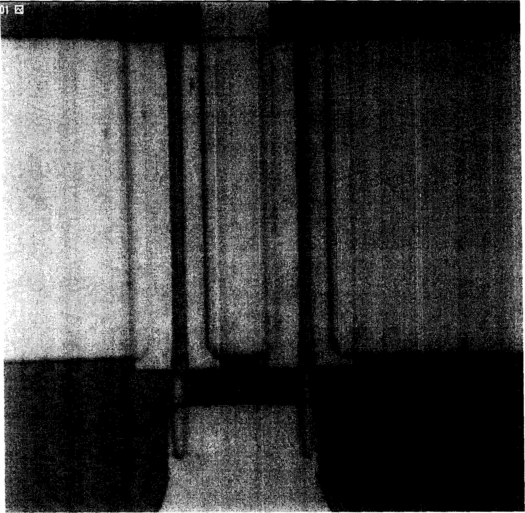
[0061] Embodiment: On the compound semiconductor experimental line of the Microelectronics Center of the Chinese Academy of Sciences, gallium arsenide (GaAs)-based MHEMT and indium phosphide (InP)-based devices were fabricated, and the method of the present invention was used to expose and develop the grid , a T-shaped gate with a gate length of 122 nanometers was obtained, and a device with good performance was obtained.
[0062] figure 2 It is a photo of the device actually produced.
Login to View More PUM
 Abstract
The invention discloses a circuit-T grid preparing method of high-electron mobility transistor, which comprises the following steps: preparing primitive substrate; cleaning; marking; preparing separation island; evaporating source-drain metal; stripping; alloying; cleaning the substrate; coating PMMA glue; baking; fetching the substrate; exposing the glued substrate through electron beam; developing PMMA glue on the substrate; fixing image; blowing. The method is compatible with advantages of present two T-typed grid preparing method, which avoids each defect simultaneously.
Description
technical field [0001] The invention relates to the technical field of ultra-high-speed microelectronic devices, in particular to a method for manufacturing a T-shaped gate of a high electron mobility transistor (HEMT) circuit. Background technique [0002] Indium phosphide (InP)-based and gallium arsenide (GaAs)-based compound semiconductor materials are not only excellent optoelectronic materials, but also ideal ultra-high-speed microelectronic materials, which have broad applications in optical communications, satellite communications, mobile communications, and space energy . At present, the highest oscillation frequency (f max ) up to 600GHz indium phosphide (InP)-based high electron mobility transistor (HEMT), becoming the fastest three-terminal device, the f of indium phosphide (InP)-based heterojunction transistor (HBT) max It has also reached 250GHz. It is an ideal device for the drive circuit of the transmitting module and the amplifying circuit of the receiving ...
Claims
Login to View More Application Information
Patent Timeline
 Patent Type & AuthorityApplications(China)
IPC IPC(8): H01L21/28H01L21/44H01L21/8234
Inventor张海英
OwnerSEMICON MFG INT (SHANGHAI) CORP