Pixels for cmos image sensors

An oxide semiconductor and image sensor technology, which is applied in the field of image sensors, can solve the problems of complex manufacturing process, difficult implementation, and increased manufacturing cost, so as to increase the drain-source voltage difference, improve charge transfer efficiency, and widen the The effect of dynamic range

Inactive Publication Date: 2006-11-22
SAMSUNG ELECTRONICS CO LTD
View PDF0 Cites 16 Cited by
  • Summary
  • Abstract
  • Description
  • Claims
  • Application Information

AI Technical Summary

Problems solved by technology

However, the method is not easy to implement because it is difficult to form a floating diffusion junction (or a floating diffusion region) since the electrode of the transfer gate extends into the floating diffusion region.
[0014] That is, it is difficult to form the floating diffusion region using the gate self-aligning ion implantation technique
Therefore, when the transfer gate is formed after the floating diffusion region is formed, additional photomask processing is required, so the manufacturing process becomes more complicated and the manufacturing cost increases
In addition, since it is difficult to design and control the channel width of the transfer transistor, it is difficult to guarantee the electrical characteristics of the transfer transistor

Method used


Image

  • Pixels for cmos image sensors
  • Pixels for cmos image sensors
  • Pixels for cmos image sensors

Examples


Embodiment Construction

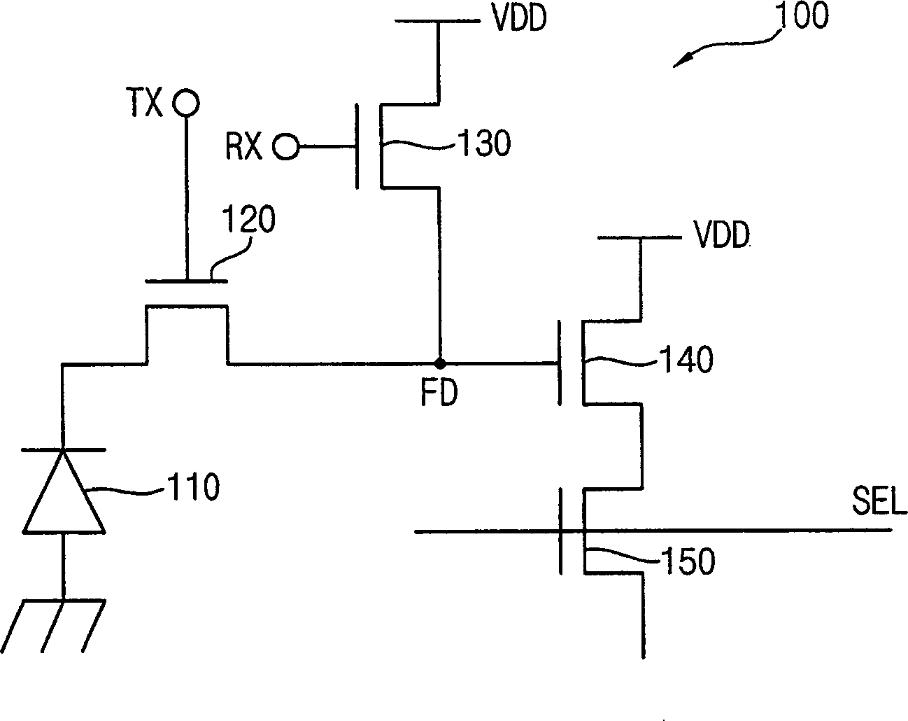
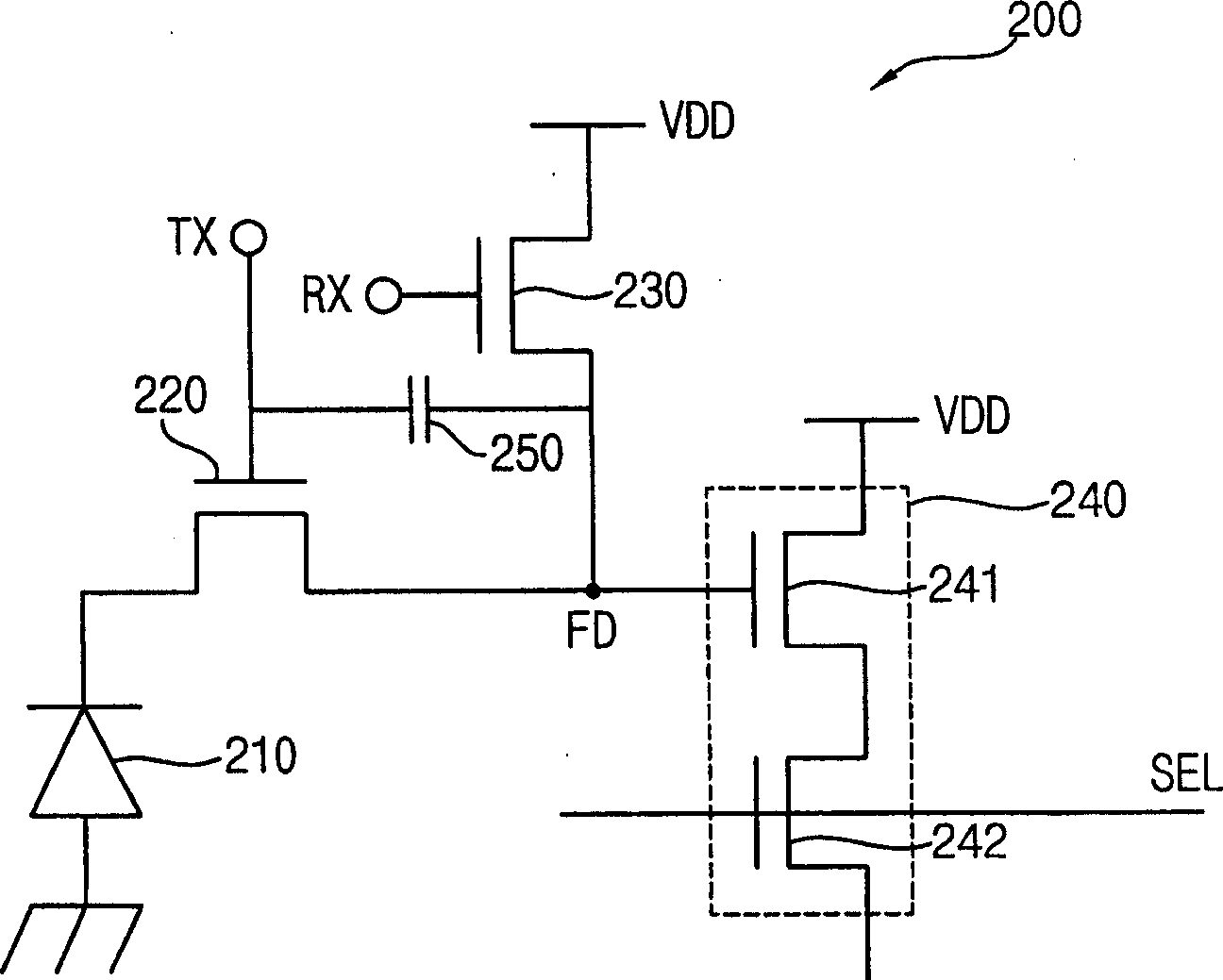
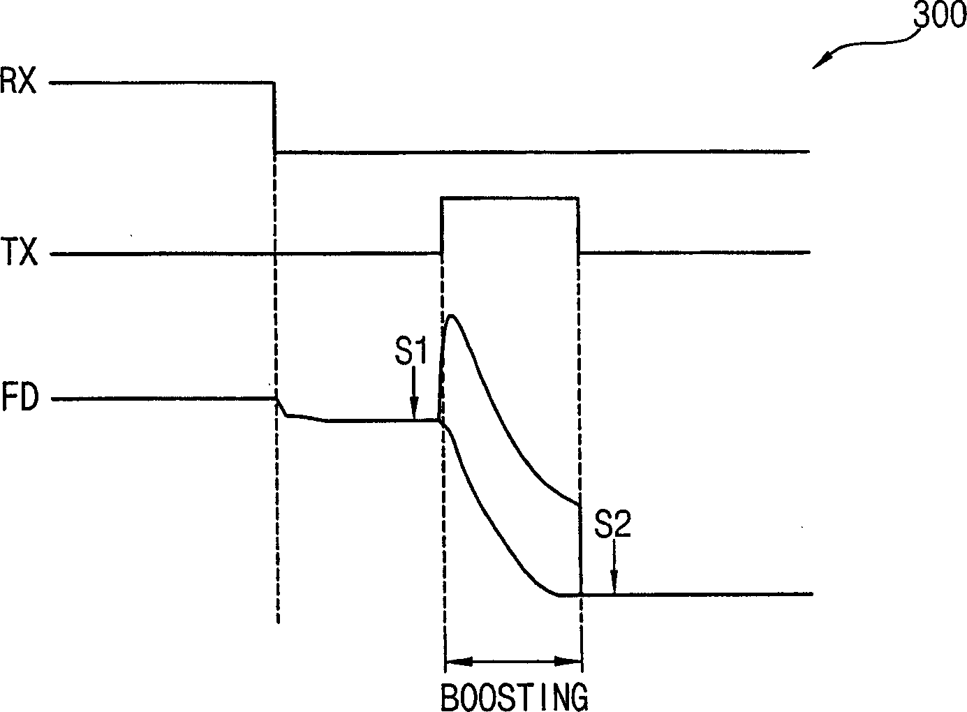
[0036] Exemplary embodiments of the present invention are disclosed herein. Specific structural and functional details shown are merely representative for purposes of describing example embodiments. Thus, the invention may be embodied in many alternative forms and should not be construed as limited to the exemplary embodiments set forth herein.

[0037] Therefore, while the invention is susceptible to various modifications and alternative forms, there are shown by way of example in the drawings specific embodiments of the invention and the same is described in detail. It should be understood, however, that the intention is not to limit the invention to the specific example forms described, but on the contrary, the invention covers all modifications, equivalents, and alternatives falling within its spirit and scope. Like reference numbers may refer to like elements throughout the description of the figures.

[0038] It will be understood that, although the terms first, second...


PUM


Abstract

A unit pixel of a complementary metal-oxide semiconductor (CMOS) image sensor includes a photoelectric conversion element, a transfer transistor, a boosting capacitor and a signal transfer circuit, where the photoelectric conversion element generates a charge based on incident light, the transfer transistor transfers the charge to a floating diffusion node in response to a transfer control signal, the boosting capacitor is disposed between a gate of the transfer transistor and the floating diffusion node, the signal transfer circuit transfers an electric potential of the floating diffusion node in response to a selection signal, and a dynamic range of the electric potential of the floating diffusion node may be widened and a drain-source voltage difference of the transfer transistor may be increased so that the charge transfer efficiency may be enhanced.

Description

technical field [0001] The present invention relates to image sensors, and more particularly to complementary metal oxide semiconductor (CMOS) image sensors. Background technique [0002] An image sensor is a semiconductor module that converts photographic images into electrical signals. Image sensors are generally widely used in digital cameras, cellular phones with built-in cameras, visual systems, and the like. [0003] There are generally two types of image sensors on the market. One is a Charge Coupled Device (CCD) type image sensor, and the other is a Complementary Metal Oxide Semiconductor (CMOS) type image sensor. CMOS type image sensors have inferior noise characteristics and image quality compared to CCD type image sensors. However, the CCD type image sensor has disadvantages in production cost and power consumption compared with the CMOS type image sensor. The CMOS type image sensor may be manufactured through a conventional semiconductor manufacturing process...

Claims


Application Information

Patent Timeline
Patent Type & Authority Applications(China)
IPC IPC(8): H01L27/146
CPCH01L27/14609H04N25/59H04N25/626H04N25/778H04N25/77H04N25/57
Inventor 金利泰金永灿孔海庆崔成浩
Owner SAMSUNG ELECTRONICS CO LTD
Why Eureka
Try Eureka