Light emitting device and electronic appliance using the same

A technology of emission device and electron, applied in lighting device, electroluminescence light source, application, etc., can solve the problem of low manufacturing margin and achieve the effect of low power consumption

Inactive Publication Date: 2006-11-22
SEMICON ENERGY LAB CO LTD
View PDF1 Cites 15 Cited by
  • Summary
  • Abstract
  • Description
  • Claims
  • Application Information

AI Technical Summary

Problems solved by technology

However, in order to realize Patent Document 1, three materials must be evaporated at the s

Method used


Image

  • Light emitting device and electronic appliance using the same
  • Light emitting device and electronic appliance using the same
  • Light emitting device and electronic appliance using the same

Examples


Embodiment approach

[0039] Although the present invention has been described in detail with reference to the accompanying drawings, it should be understood that various changes and modifications will be apparent to those skilled in the art. Therefore, unless otherwise these changes and modifications depart from the scope of the present invention, they should be construed as being included therein. Therefore, the present invention should be construed as not limited to the description of the embodiments given below.

Embodiment approach 1

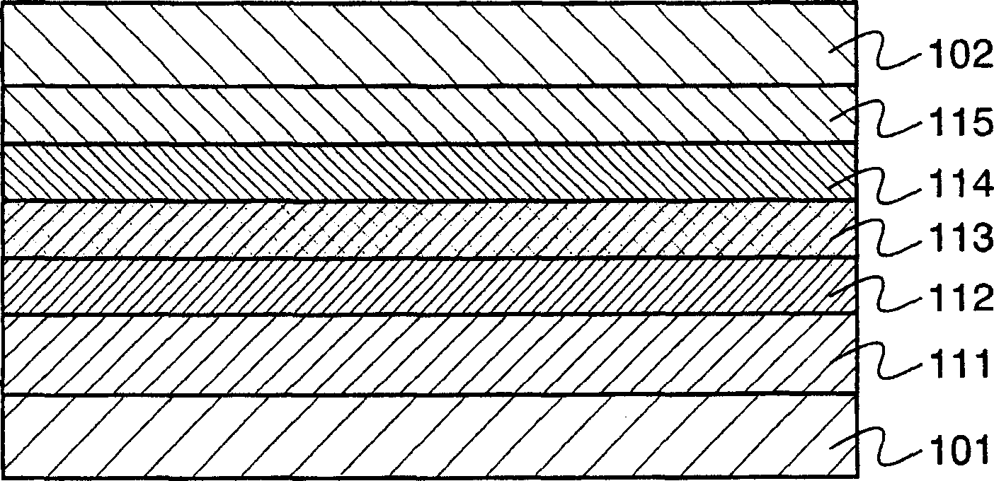
[0041] combine figure 1 One embodiment of the light-emitting element of the present invention will be described.

[0042] figure 1 A light emitting element including a light emitting layer 113 between a first electrode 101 and a second electrode 102 is shown. In addition, a first mixed layer 115 containing an electron transport substance and a substance exhibiting electron donating properties to the electron transport substance is provided between the light emitting layer 113 and the second electrode 102 . In addition, on the side of the light-emitting layer 113 close to the first electrode 101, the hole transport layer 112 in contact with the light-emitting layer 113 is formed, and on the side of the light-emitting layer 113 close to the second electrode 102, the hole transport layer 112 in contact with the light-emitting layer 113 is formed. transfer layer 114 . noticed figure 1 The light emitting element in has a hole injection layer 111 disposed between a first electro...

Embodiment approach 2

[0077] The synthesis method of the organometallic complex used in the practice of the present invention will be described below. Note that the synthesis method is not limited to the method disclosed here, and other synthesis methods may be employed.

[0078] The organometallic complex of the present invention represented by any one of Structural Formula (8) - Structural Formula (31) is obtained by a synthesis method such as represented by Synthesis Route (a-1) - Synthesis Route (a-3). Ligands with electron-withdrawing groups were synthesized via the synthetic route (a-1). Subsequently, the synthesized ligand having an electron-withdrawing group is mixed with iridium(III) chloride hydrochloride hydrate, as shown in the synthesis scheme (a-2), to coordinate the ligand to iridium. In addition, a monoanionic ligand is coordinated to iridium as shown in the synthetic scheme (a-3).

[0079]

[0080]

[0081] Here, R in the synthetic route (a-1) to the synthetic route (a-3) ...


PUM

PropertyMeasurementUnit
Thicknessaaaaaaaaaa
Thicknessaaaaaaaaaa
Thicknessaaaaaaaaaa

Abstract

The light emitting element includes a first electrode and a second electrode, between which a light emitting layer, a hole transporting layer provide in contact with the light emitting layer, an electron transporting layer provided in contact with the light emitting layer, and a mixed layer provided between the electron transporting layer and the second electrode. The mixed layer includes an electron transporting substance and a substance showing an electron donating property with respect to the electron transporting substance. The light emitting layer includes an organometallic complex represented in General Formula (1) and a host. R1 and R2 each represent an electron-withdrawing substituent group. R3 and R4 each represent any of hydrogen or an alkyl group having 1 to 4 carbon atoms. L represents any of a monoanionic ligand having a beta-diketone structure, a monoanionic bidentate chelating ligand having a carboxyl group, or a monoanionic bidentate chelating ligand having a phenolic hydroxyl grou

Description

technical field [0001] The present invention relates to a light-emitting element capable of obtaining light emission from a tertiary excited state, and a light-emitting device and electronic equipment using the light-emitting element. Background technique [0002] A light-emitting element that emits light when excitons generated by recombination of holes and electrons between a pair of electrodes returns to a ground state can be used as a pixel or a light source. Therefore, its development has gradually deepened in recent years. In the study of light-emitting elements, for light-emitting devices using light-emitting elements as pixels or lighting devices using light-emitting elements as light sources, it is important to improve light emission efficiency to reduce energy consumption of light-emitting devices. [0003] It has previously been known that light emission efficiency can be improved by using phosphorescent substances. For example, in Patent Document 1 (PCT Interna...

Claims


Application Information

Patent Timeline
IPC IPC(8): H01L51/50C09K11/06H01L51/54H05B33/14
CPCC09K11/06C09K2211/1022C09K2211/1029C09K2211/1044C09K2211/185H05B33/14Y10S428/917C09K11/025H10K85/361H10K85/342H10K50/155H10K50/11H10K2101/10H10K50/165H10K85/6572C09K2211/1007
Inventor 大澤信晴井上英子瀬尾哲史下垣智子
Owner SEMICON ENERGY LAB CO LTD
Why Eureka
Try Eureka