

Multilayer mirror, method for manufacturing the same, and exposure equipment
A multi-layer film and reflector technology, which is applied in photolithography exposure devices, microlithography exposure equipment, semiconductor/solid-state device manufacturing, etc., can solve problems such as failure to reach
- Summary
- Abstract
- Description
- Claims
- Application Information
AI Technical Summary
Problems solved by technology
Method used
Image

Examples
Embodiment 1
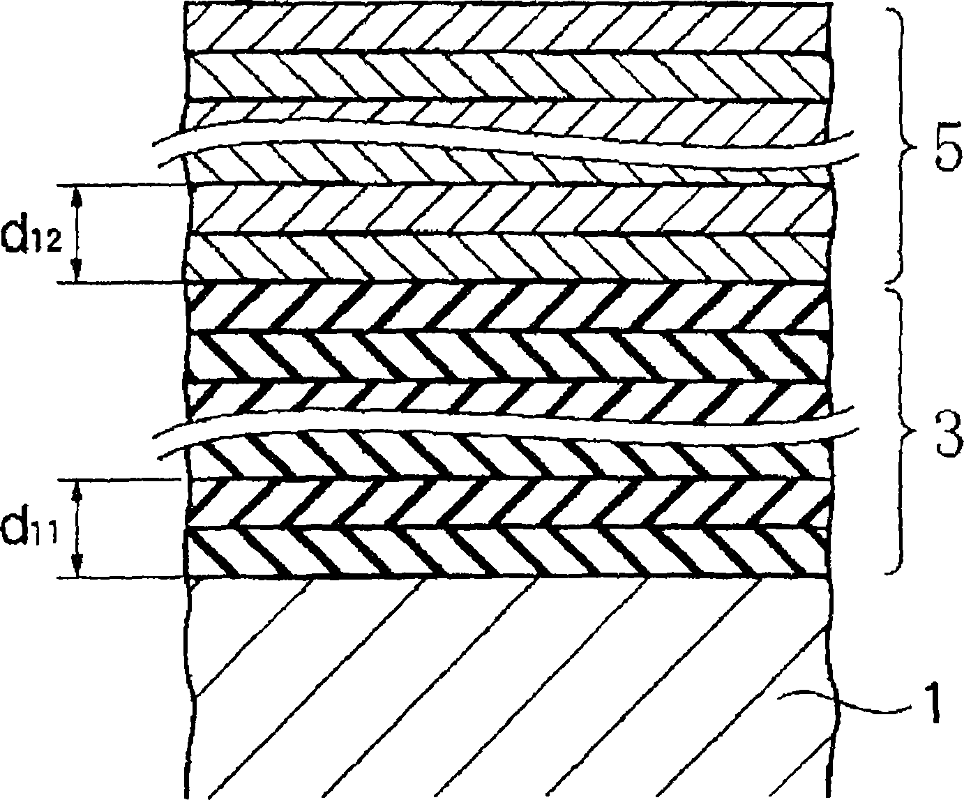
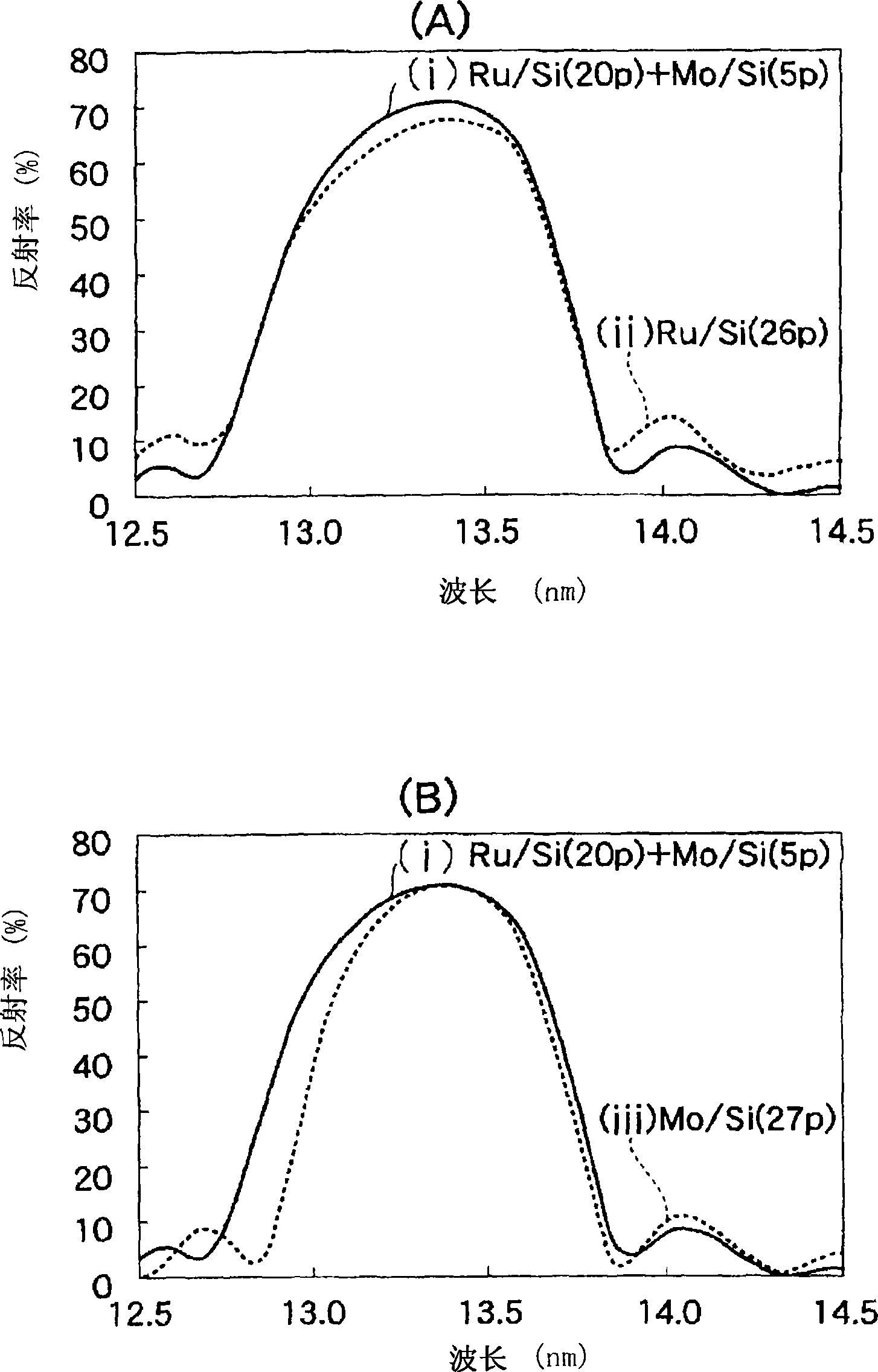
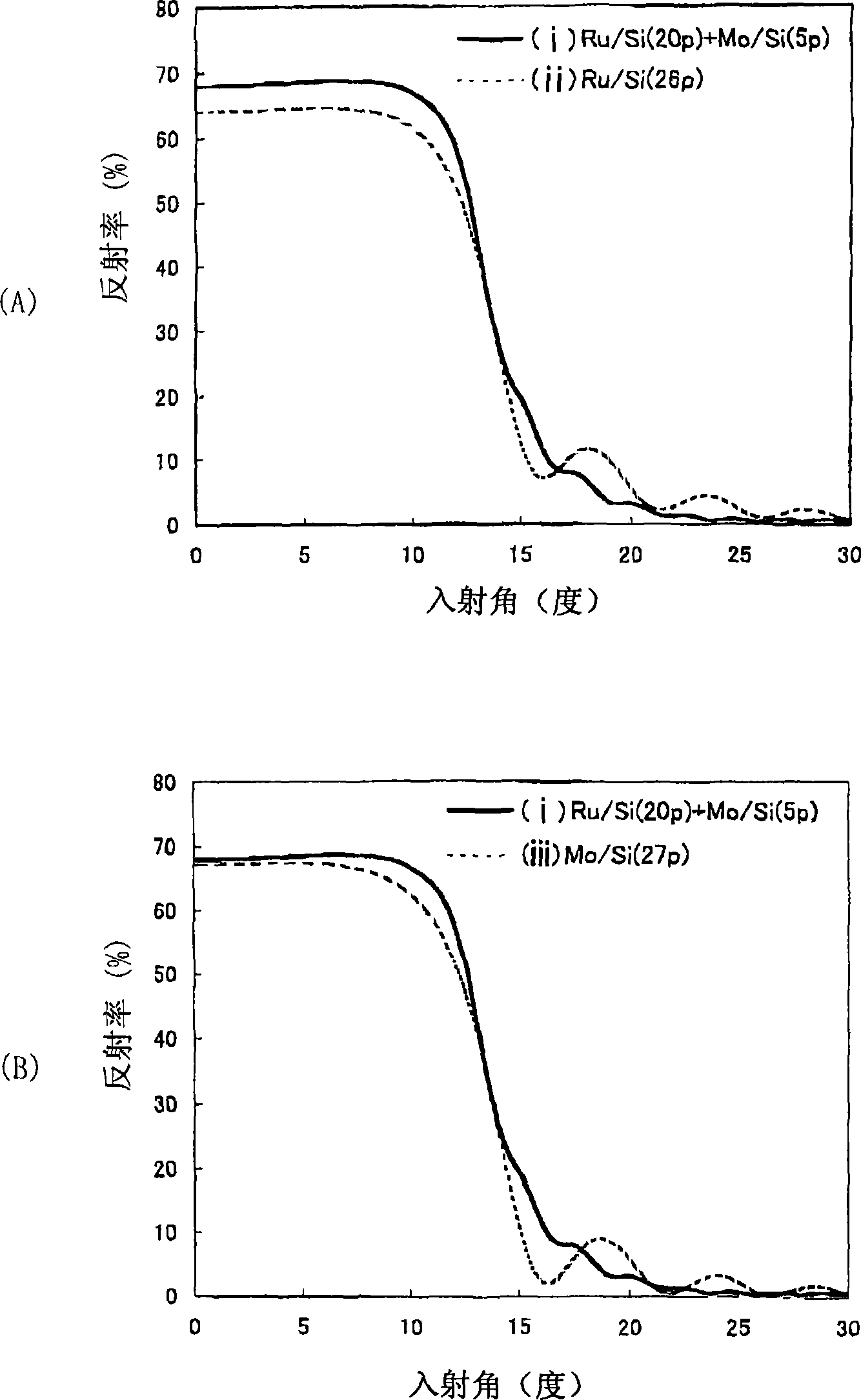
[0126] figure 1 is a cross-sectional view of the multilayer film mirror according to the first embodiment of the present invention. The substrate 1 is made of low thermal expansion glass polished to a surface roughness of 0.2 nm RMS or less. Twenty pairs of Ru / Si multilayer films 3 are formed on the surface of the substrate 1 , and five pairs of Mo / Si multilayer films 5 are formed on the Ru / Si multilayer films 3 . The period length of the Ru / Si multilayer film 3 (the thickness of the unit periodic structure (film layer pair) of Ru / Si, is represented by d in the figure 11 Expressed) is 6.86nm, and the period length of Mo / Si multilayer film 5 (thickness of the film layer pair of Mo / Si, denoted by d in the figure 12 Expressed) is 6.9nm. The Γ value of these multilayer films in each unit periodic structure is 0.4. Note that the Γ value is the thickness of the Ru layer or Mo layer (d Ru or d Mo ) to the ratio of the period length (d) of the multilayer film (Γ=d Ru / d or Γ=d...
Embodiment 2
[0133] Figure 4 is a schematic cross-sectional view of a multilayer film mirror according to the second embodiment of the present invention. The substrate 10 is made of low thermal expansion glass polished to a surface (top surface in the figure) roughness of 0.2 nm RMS or less. Four pairs of Mo / Si multilayer films (deep film layer group) 11 are formed on the surface of the substrate 10 . The period length of the Mo / Si multilayer film 11 (the thickness of the Mo / Si film layer pair) was 6.9 nm, and the Γ value was 0.5.
[0134] On the surface of the Mo / Si multilayer film 11 is formed an additional layer 12 (a silicon layer in this embodiment). The thickness of the additional layer 12 is adjusted so as to have an optical thickness of about 1 / 4 of the wavelength of the incident light. In this embodiment, the thickness of the additional layer 12 is about 3.5 nm. In addition, on the surface of the additional layer 12, 20 pairs of Mo / Si multilayer films (surface film layer grou...
Embodiment 3
[0141] Image 6 is a schematic cross-sectional view of a multilayer film mirror according to a third embodiment of the present invention. The substrate 20 is made of low thermal expansion glass polished to a surface (top surface in the figure) with a roughness of 0.2 nm RMS or less. Five pairs of Ru / Si multilayer films (deep film layer group) 21 are formed on the surface of the substrate 20 . The period length of the Ru / Si multilayer film 21 (the thickness of the Ru / Si film layer pair) is 6.9 nm, and the Γ value is 0.5.
[0142] On the surface of the Ru / Si multilayer film 21 is formed an additional layer 22 (a silicon layer in this embodiment). The thickness of the additional layer 22 is adjusted to have an optical thickness of about 1 / 4 of the wavelength of the incident light. In this embodiment, the thickness of the additional layer 22 is about 3.85 nm. In addition, on the surface of the additional layer 22, 20 pairs of Ru / Si multilayer films (surface film layer groups) ...
PUM
| Property | Measurement | Unit |
|---|---|---|
| Wavelength | aaaaa | aaaaa |
| Half width | aaaaa | aaaaa |
| Thickness | aaaaa | aaaaa |
Abstract
Description
Claims
Application Information