Doping agent for dielectric material of ceramic capacitor, dielectric material, and preparation method
A technology of ceramic capacitors and dielectric materials, which is applied in the direction of fixed capacitor dielectrics, ceramics, and parts of fixed capacitors. It can solve problems such as environmental impact, lower sintering temperature, and harm, and achieve low firing temperature, small dielectric loss, and The effect of simple preparation process
- Summary
- Abstract
- Description
- Claims
- Application Information
AI Technical Summary
Problems solved by technology
Method used
Image
Examples
preparation example Construction
[0064] The method that the present invention proposes to prepare the nano-dopant of described ceramic material is as follows (referred to as process method 1):
[0065] The initial raw materials include inorganic compounds and organic compounds: inorganic compounds include rare earth oxides (Nd, and oxides of elements such as Y, La, Ce, Pr, Sm, Gd, Dy, Ho, Er, Lu, or Yb), alkali / alkaline earth Metal carbonate Na 2 CO 3 , Li 2 CO 3 , Mg(OH) MgCO 3 ·5H 2 O, CaCO 3 , SrCO 3 、BaCO 3 , the boron compound Na 4 B 4 o 7 or H 3 BO 3 , transition metal nitrate Mn(NO 3 ) 2 , Co(NO 3 ) 2 ·6H 2 One or more of O, etc. and concentrated nitric acid solution. Organic compounds include ethyl orthosilicate, acetylacetone, and absolute ethanol, all of which are analytically pure.
[0066] The specific process of preparing this nanoscale ceramic material additive is as follows: (the following raw materials and process parameters are only for illustration)
[0067] ①. Weigh rare...
Embodiment 1
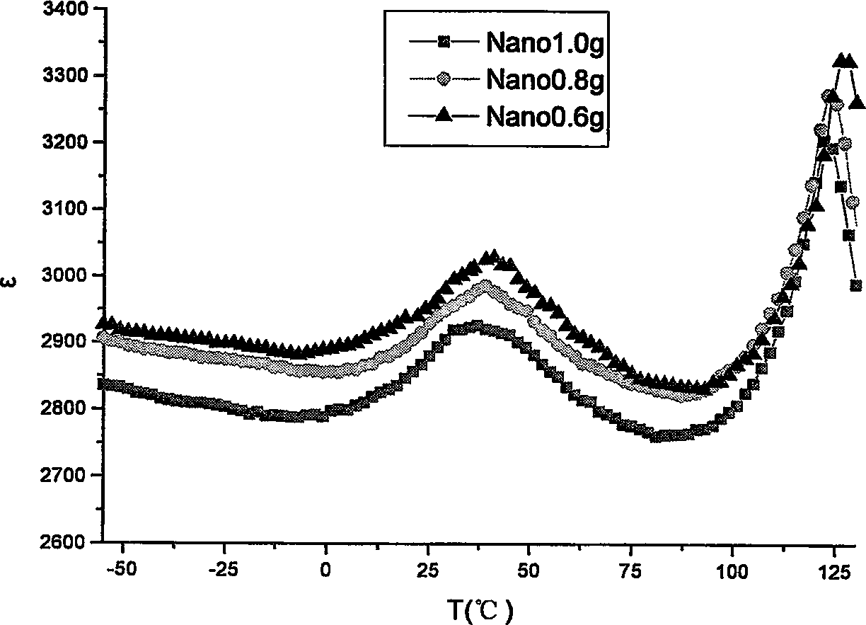
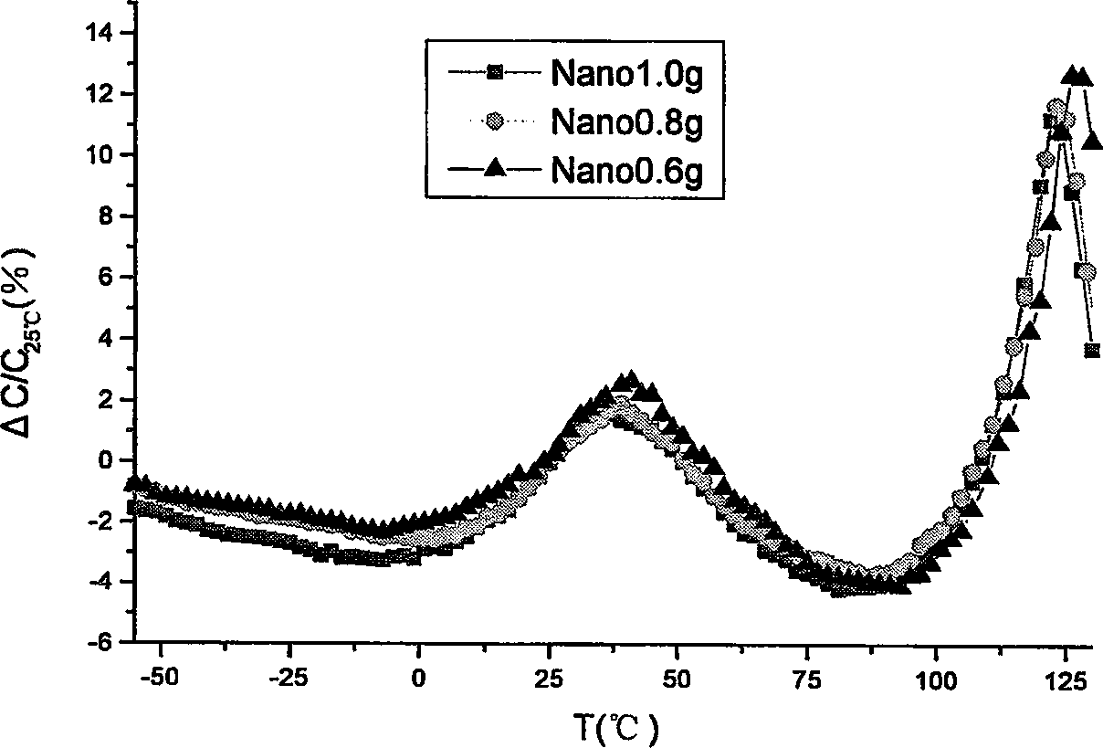
[0094] Example 1: (Comparison of dosages of different nano-dopants) Process method 2 was used to prepare ultra-fine medium-temperature sintering and temperature-stable multilayer ceramic capacitor dielectric materials. According to BaTiO 3 : 97.5mol% (grain size is 50nm), 0.8mol% Nb 2 o 5 , 1.1mol% ZnO, 0.6mol% CeO 2 Proportioning and weighing. The nano-dopants (abbreviated as Nano) in samples of the nano-additives prepared in Example 1 of the present invention were 1.0 g, 0.8 g, and 0.6 g, respectively. After the obtained sample was dried, it was mixed with 5wt% PVA and granulated, and pressed under a pressure of 10 MPa to form a disc with a diameter of 10 mm and a thickness of 1 mm, and then placed in the air for sintering at a temperature of 1140° C. for 2.5 hours. The heating rate was 3°C / min, and the furnace was cooled. The dielectric properties of the obtained ceramic samples are shown in Table 1. Figure 1 ~ Figure 2 The ε-T curves and ΔC / C curves of different dosa...
Embodiment 2
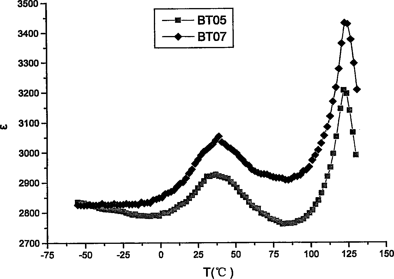
[0096] Example 2: (Comparison of BT particle size) Process method 2 was used to prepare ultra-fine medium-temperature sintering temperature-stable multilayer ceramic capacitor dielectric material. According to 97.3wt% BaTiO 3 (grain size 50nm and 70nm, respectively), 1.01wt% Nb 2 o 5 , 0.3wt% ZnO, 0.45wt% CeO 2 , 0.94wt% Nano proportioning and weighing. Ball milling, after drying, add 5wt% PVA to mix and granulate, press to form a disc with a diameter of 10mm and a thickness of 1mm under a pressure of 10Mpa, and then sinter in air at a sintering temperature of 1140°C, keep warm for 2.5 hours, and heat up The rate is 3°C / min, and the dielectric properties of the obtained ceramic samples are shown in Table 2. Figure 3 ~ Figure 4 The BaTiO with different particle sizes are given respectively 3 (abbreviated as BT) ε-T curve and ΔC / C 25℃ -T curve.
[0097] No.
PUM
| Property | Measurement | Unit |
|---|---|---|
| Particle size | aaaaa | aaaaa |
| Grain size | aaaaa | aaaaa |
Abstract
Description
Claims
Application Information


