Strain source-drain CMOS integrating method with oxide separation layer

An integrated method and oxide technology, applied in electrical components, semiconductor/solid-state device manufacturing, circuits, etc., can solve problems such as erosion of spacers and shallow trench isolation regions, and achieve wide process tolerance, safe removal, and easy process. Effect

Active Publication Date: 2007-01-10
SEMICON MFG INT (SHANGHAI) CORP +1
View PDF0 Cites 25 Cited by
  • Summary
  • Abstract
  • Description
  • Claims
  • Application Information

AI Technical Summary

Problems solved by technology

[0004] The purpose of the present invention is to overcome the problem of corroding spacers and shallow trench isolation regions when removing polysilicon hard masks in the prior art, and to provide CMOS with oxide spacers and strained source and drain, that is, PMOS and epitaxial growth of silicon germanium. Method for growing silicon-carbon NMOS fabrication integrated with safe hardmask removal process

Method used


Image

  • Strain source-drain CMOS integrating method with oxide separation layer
  • Strain source-drain CMOS integrating method with oxide separation layer
  • Strain source-drain CMOS integrating method with oxide separation layer

Examples


Embodiment 1

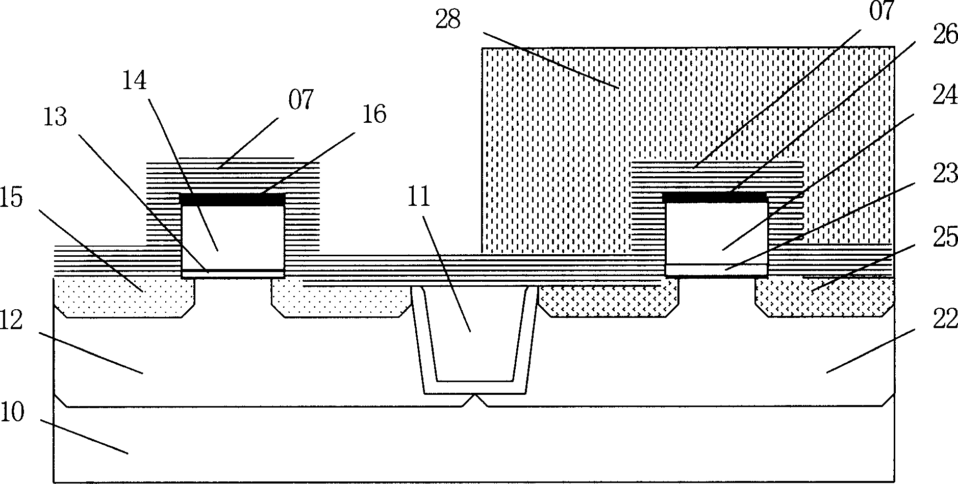
[0066] Such as Figure 3a As shown, the NMOS region is protected with a photoresist 28, and the photolithographic patterning exposes the PMOS region. Such as Figure 3b As shown, the spacer layer 17 of the PMOS region is then etched to form the spacer layer 17 of the PMOS region, and the NMOS region is protected.

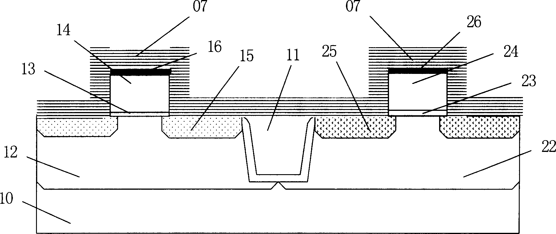
[0067] Such as Figure 4 As shown, the photoresist 28 in the NMOS area is removed and cleaned, and the PMOS polysilicon hard mask 16 and the spacer layer 17 are used as a photolithography pattern mask to conduct self-aligned silicon substrate recess etching in the PMOS area. A silicon germanium layer 155 is epitaxially grown on the recessed silicon. Its germanium concentration is 5-45%. Then chemical vapor deposition of nitride 09 with a thickness of 50-500 Å is carried out in the PMOS region and the NMOS region. As shown in Table 2, since silicon has a higher etching rate than silicon nitride, its etching rate ratio is 4-5.4, so it is easy to realize and contr...

Embodiment 2

[0074] The above PMOS and NMOS epitaxial growth sequences can be interchanged, and the method is the same as before, that is, the NMOS silicon carbon is first formed before the silicon germanium is formed.

[0075] The PMOS area is protected with photoresist, and the NMOS area is exposed by photolithography patterning. Then, the spacer layer of the NMOS region is etched to form the spacer layer of the NMOS, and the PMOS region is protected.

[0076] The photoresist is removed and cleaned, and the polysilicon hard mask and the spacer layer are used as the mask of the photolithographic pattern, and the self-aligned silicon substrate is recessed and etched in the NMOS region. Silicon carbon is grown on the recessed silicon. Its carbon concentration is 0.5-10%. Silicon nitride with a thickness of 50-500A is chemically vapor deposited in the PMOS and NMOS regions.

[0077] The NMOS area is covered with photoresist, and a photoresist pattern is formed on the exposed PMOS area. U...


PUM


Abstract

The integration methods include following integrated parts: method for manufacturing PMOS of epitaxial growth of source and drain poles on silicon germanium by using interval layer of oxide and hard mask of polysilicon as mask; method for manufacturing NMOS of epitaxial growth of source and drain poles on silicon carbon; and removing hard mask safely. The method produces strain source and drain CMOS with interval layer of oxide.

Description

technical field [0001] The invention relates to a CMOS manufacturing method, in particular to an integration method of a strained source-drain CMOS with an oxide spacer layer. Background technique [0002] The fabrication process of an integrated circuit includes the formation of a gate pattern of a conductive structure, usually with polysilicon as the gate. In this process, the polysilicon layer is deposited on the substrate, and the single crystal silicon undergoes multiple processes such as implantation and gate oxidation. The polysilicon is then covered with a silicon oxide and / or silicon oxynitride dielectric material. The dielectric layer is photolithographically patterned and etched to form a gate conductive structure pattern. The patterned dielectric material acts as a hard mask to transfer the pattern onto the polysilicon by plasma etching. The hard mask is removed by wet chemicals after polysilicon patterning. [0003] As the critical dimensions become smaller ...

Claims


Application Information

Patent Timeline
Patent Type & Authority Applications(China)
IPC IPC(8): H01L21/8238
Inventor 朱蓓宁先捷
Owner SEMICON MFG INT (SHANGHAI) CORP
Why Eureka
Try Eureka