Semiconductor element and formation method

A semiconductor and component technology, applied in the field of semiconductor components, can solve problems such as difficult control, and achieve the effect of reducing time and cost

Inactive Publication Date: 2007-02-14
TAIWAN SEMICON MFG CO LTD
View PDF0 Cites 10 Cited by
  • Summary
  • Abstract
  • Description
  • Claims
  • Application Information

AI Technical Summary

Problems solved by technology

But in smaller designs, for example, when the design compensation spacer is less than 100 Angstroms, the traditional compensation spacer will be difficult to control

Method used


Image

  • Semiconductor element and formation method
  • Semiconductor element and formation method
  • Semiconductor element and formation method

Examples


Embodiment Construction

[0033] In order to make the above-mentioned and other objects, features, and advantages of the present invention more obvious and understandable, the preferred embodiments are specifically cited below, together with the accompanying drawings, and are described in detail as follows:

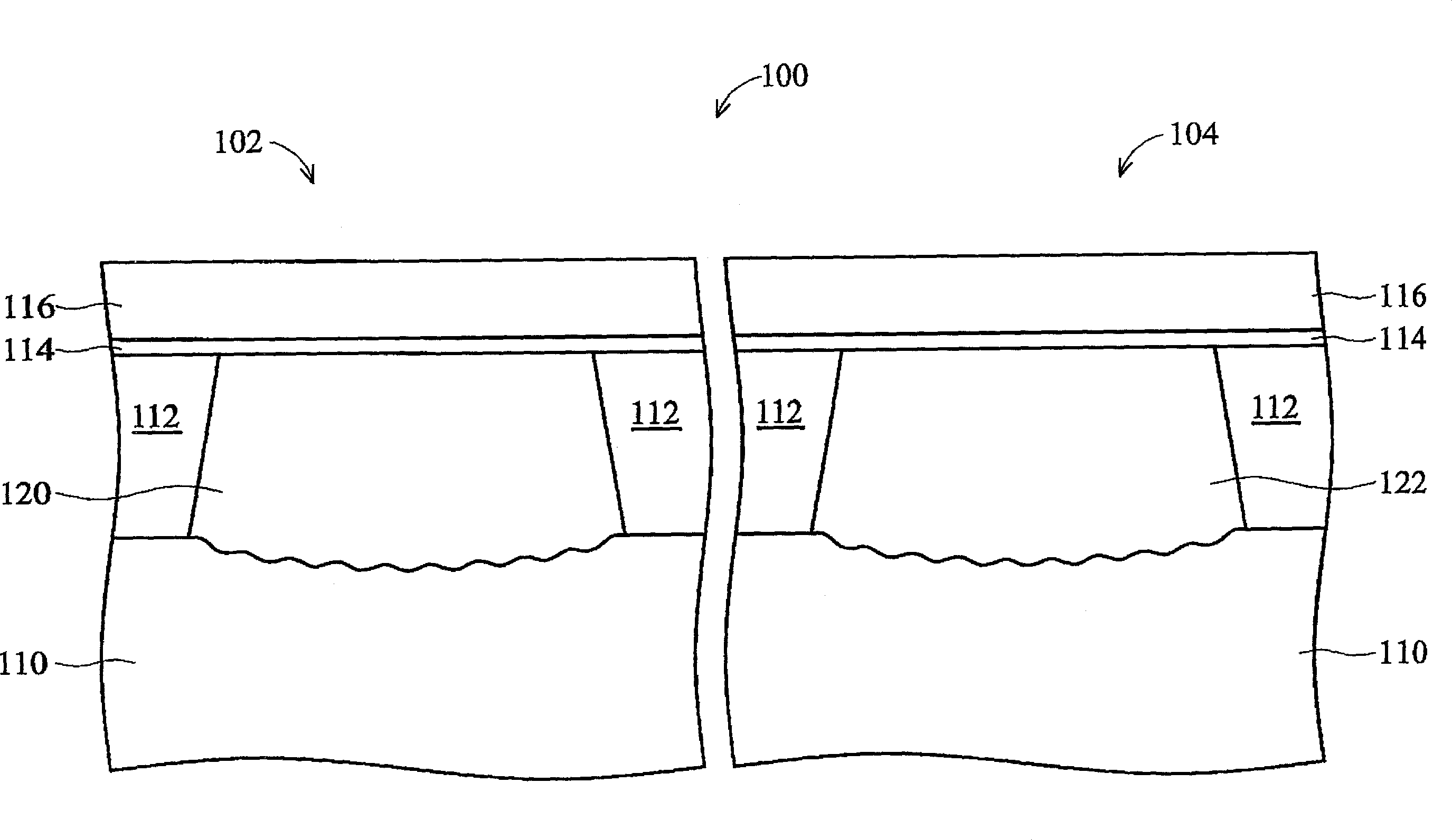
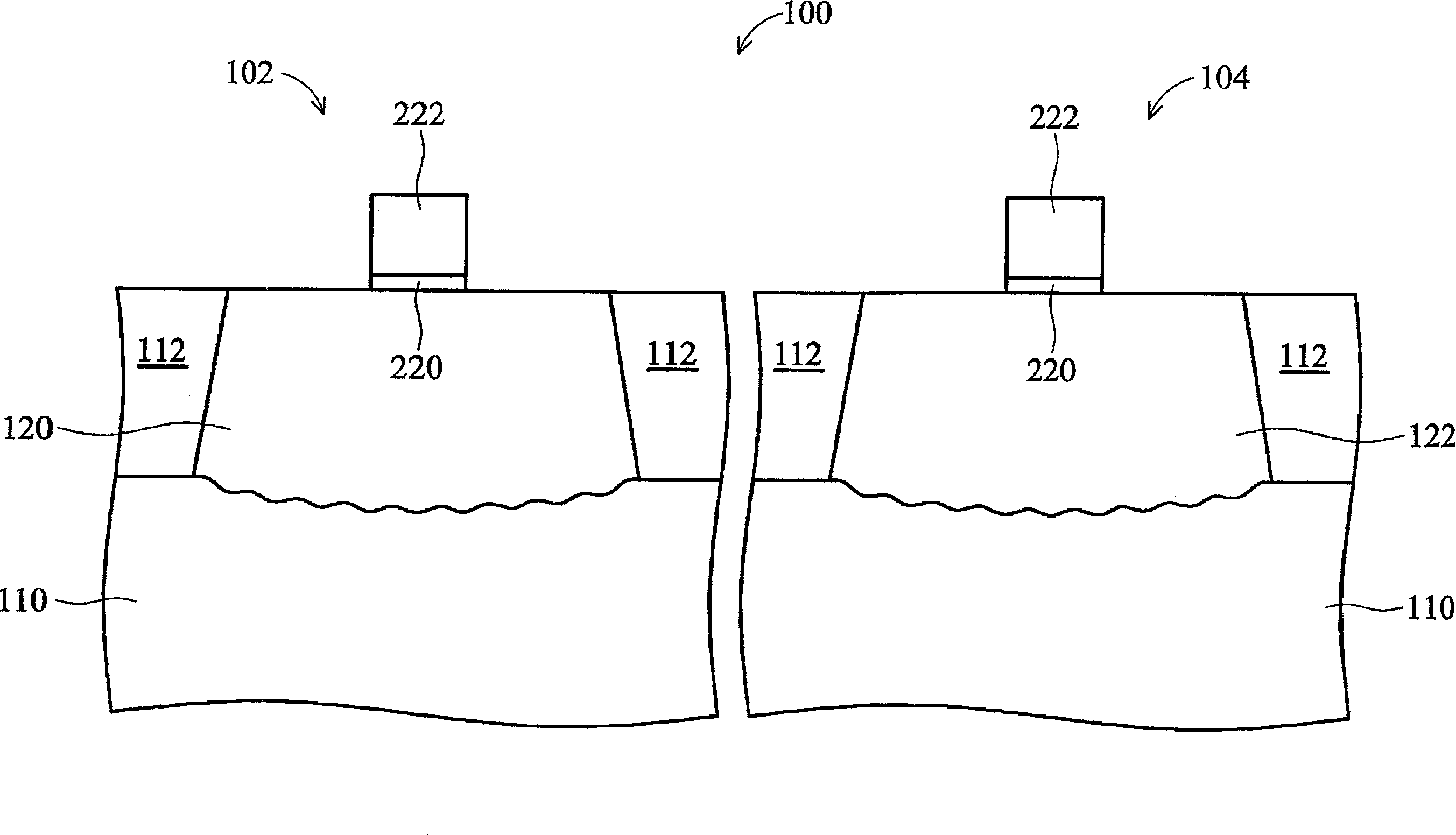
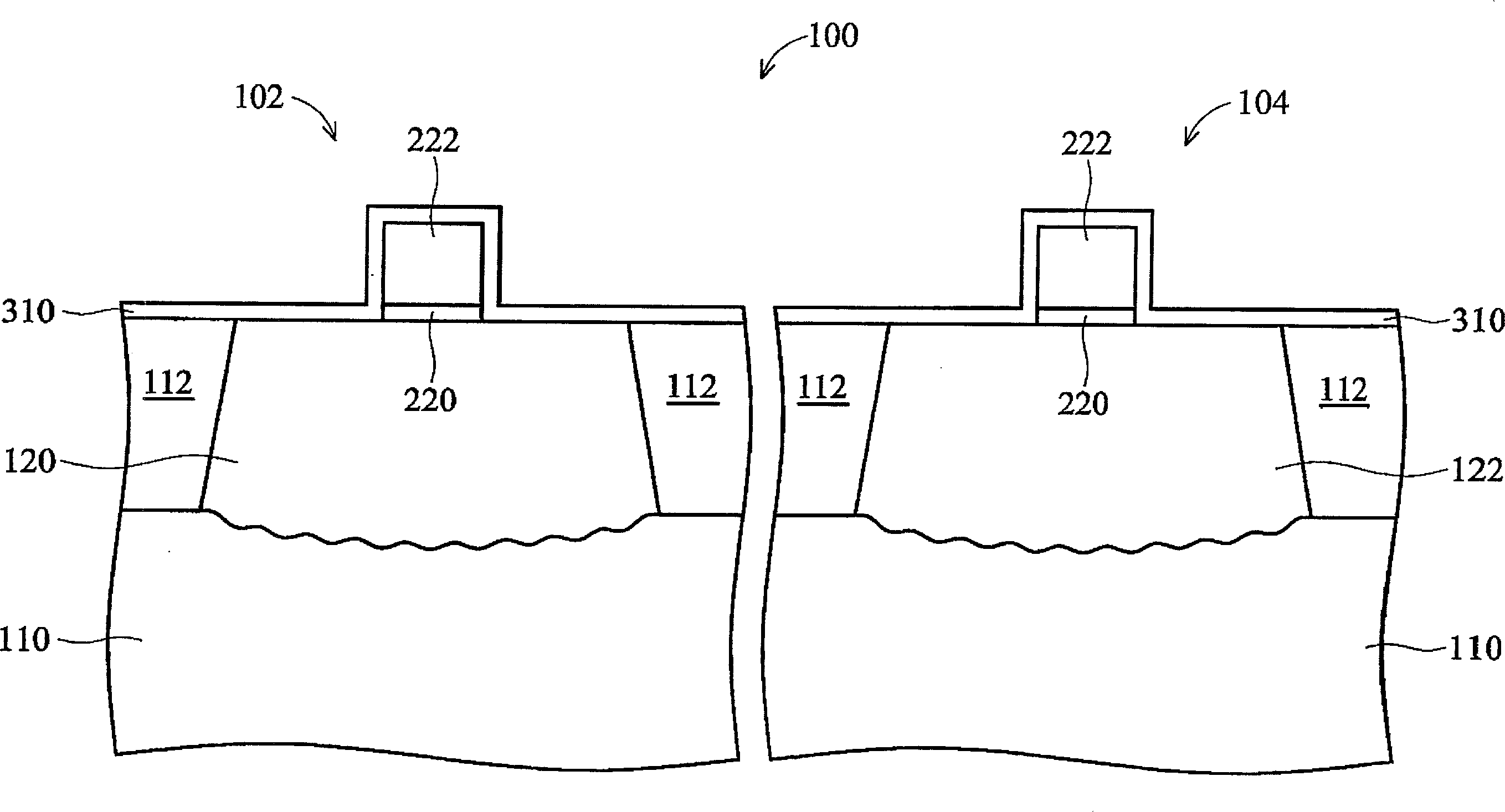
[0034] Figure 1 to Figure 6 It is shown that the present invention utilizes compensating spacers to fabricate an NMOS and a PMOS. The present invention can be applied to various circuits. For example, I / O components, core components, memory components, system-on-chip (SoC) components, or other integrated circuits. The invention can be generally applied to the process below 65 nanometers where the short channel effect often occurs.

[0035] see figure 1 , the wafer 100 includes a substrate 110 having an NMOS region 102 and a PMOS region 104 . In this embodiment, the substrate 110 includes a P-type bulk silicon substrate, a P-type well 120 is formed in the NMOS region 102 and an N-type well 122...


PUM


Abstract

The present provides a semiconductor element and a forming method thereof. An offset spacer for CMOS transistors and a method of manufacture are provided. A gate electrode is formed on a substrate, and an offset mask layer is formed over the surface of the gate electrode and the substrate. The offset mask may be formed of an oxide layer and acts as a mask during implanting, such as pocket implants and lightly-doped drain implants. A second implant spacer may be formed on top of the offset mask layer adjacent to the gate electrode, and another implant process may be performed to form deeply-doped drain regions. The semiconductor element and the forming method thereof reduces the time and cost spent in depositing and cleaning, besides, the usage of offset mask is controlled more easily.

Description

technical field [0001] The present invention relates to semiconductor components, in particular to compensation spacers for CMOS transistors. Background technique [0002] Complementary Metal Oxide Semiconductor Transistor (CMOS) technology is commonly used today in VLSI. Over the past decade, the shrinking of semiconductor dimensions has led to increases in speed, performance, and circuit density, as well as reductions in cost. The continuous reduction of CMOS size is still the main challenge. [0003] For example, reducing the length of the gate in CMOS, when the gate length is less than 30 nanometers, will increase the interaction between the source / drain region and the channel, and enhance the influence on the channel potential and gate dielectric layer, resulting in The gate electrode is unstable when controlling switching. The phenomenon of reduced gate control caused by a short channel is called the short channel effect. [0004] An existing method to reduce the s...

Claims


Application Information

Patent Timeline
Patent Type & Authority Applications(China)
IPC IPC(8): H01L21/336H01L21/266H01L29/78
CPCH01L21/823814H01L29/1083H01L21/823864H01L29/6656H01L21/823807H01L29/6659
Inventor 黄健朝
Owner TAIWAN SEMICON MFG CO LTD
Why Eureka
Try Eureka