

Target assembly and sputtering device with target assembly
A technology of assembly and bonding surface, applied in the field of sputtering device and target assembly, can solve the problems of inability to form film, melting of bonding material, exudation, etc., and achieve the effect of preventing abnormal discharge and good film formation.
- Summary
- Abstract
- Description
- Claims
- Application Information
AI Technical Summary
Problems solved by technology
Method used
Image

Examples
Embodiment approach 1
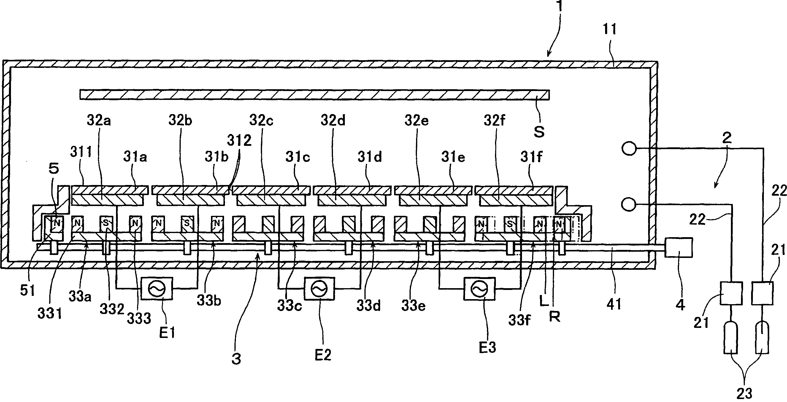
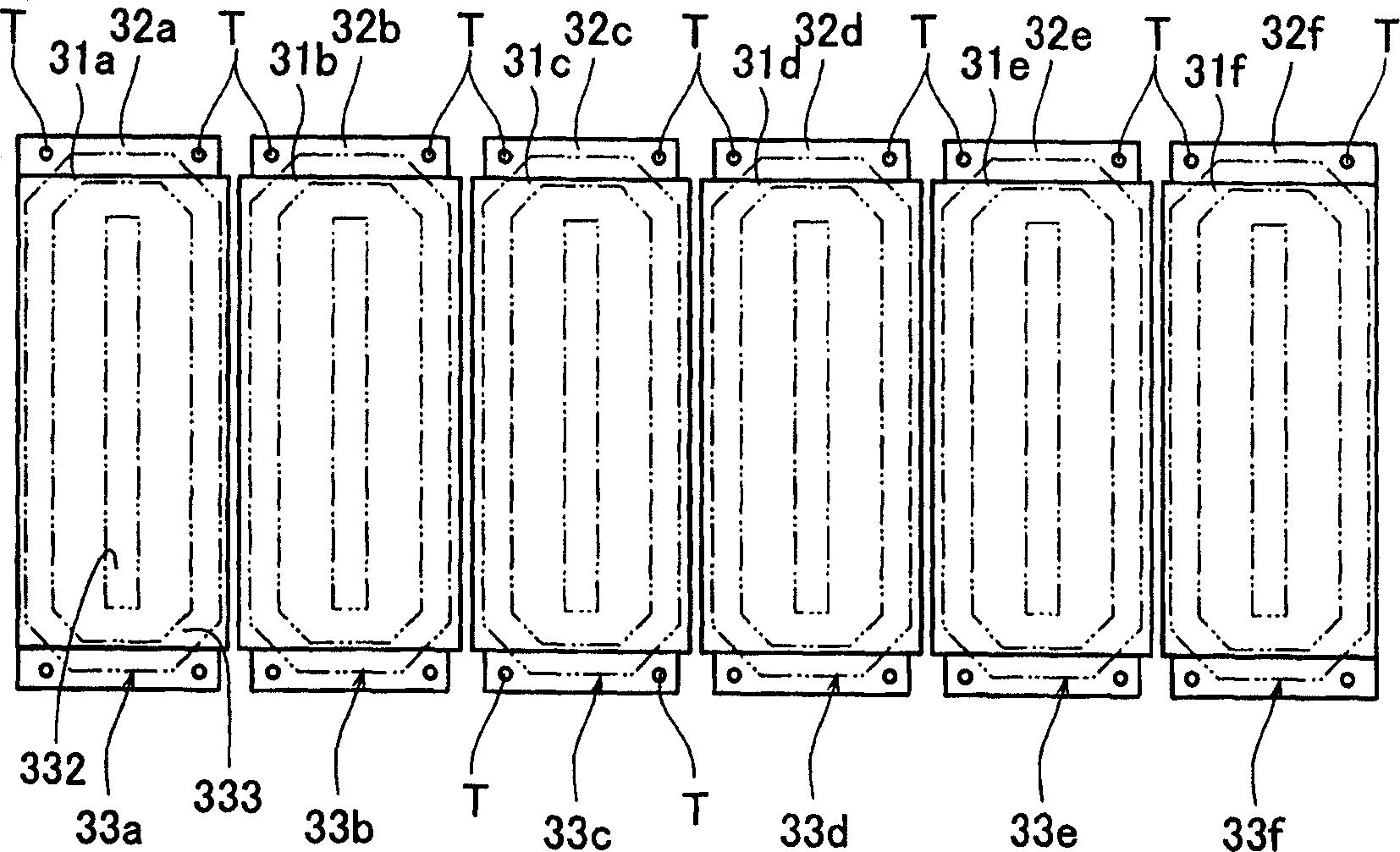
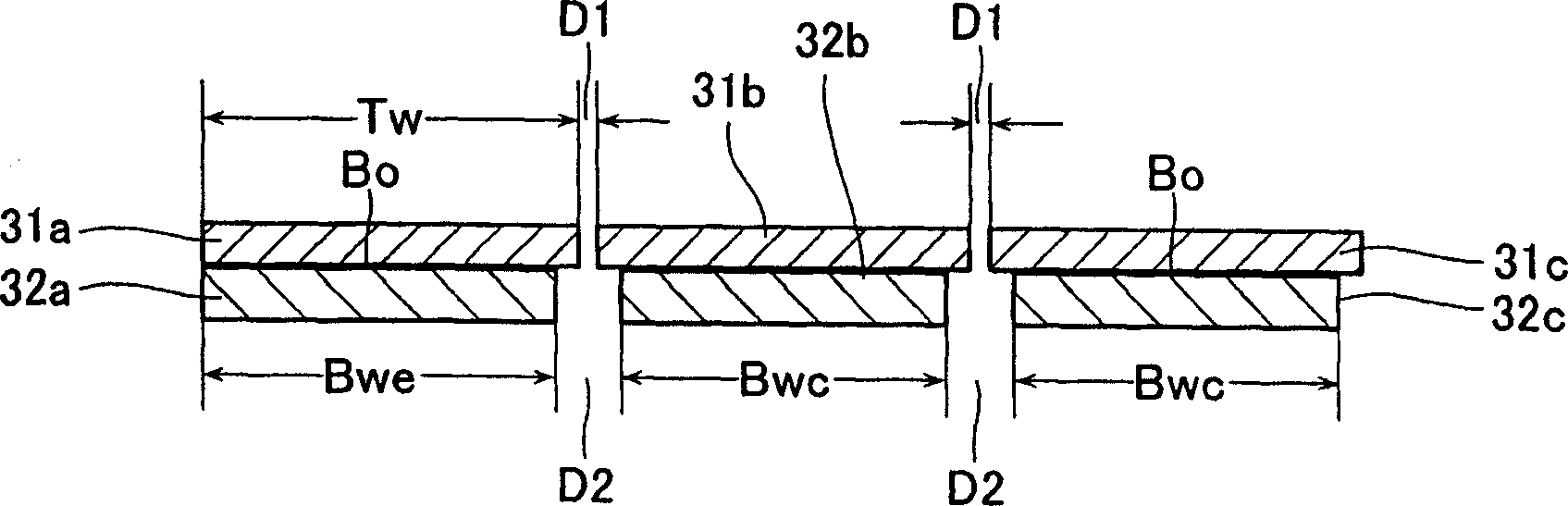
[0047] In this embodiment, using figure 1 In the shown sputtering apparatus, a glass substrate (1000 mm×1200 mm) is used as a processing substrate S, and the glass substrate is transported to a position facing the targets 31 a to 31 f by a substrate transport unit. Using Al as the targets 31a-31f, each target 31a-31f is made into a cuboid with an external dimension of 200mm×1700mm and a thickness of 10mm by a known method, and is respectively bonded to the back plates 32a-32f as a target assembly.
[0048] At this time, using In as the bonding material, when installing the target assemblies 31 and 32 on the cathode assembly 3, the distance D1 between the targets 31a to 31f is set to 2 mm, and the distances D2 and D3 between the back plates are set to 10 mm. . Moreover, the distance between target 31a-31f and a glass substrate was set to 160 mm.
[0049] As sputtering conditions, the pressure in the evacuated vacuum chamber 11 was maintained at 0.3 Pa, and the mass flow contr...
PUM
 Abstract
Description
Claims
Application Information