Nitride semiconductor vertical cavity surface emitting laser

A technology of vertical cavity surface emission and nitride semiconductor, which is applied in the direction of semiconductor lasers, lasers, laser components, etc., can solve the problems of limiting optical gain performance, and achieve the effects of low heat generation, high optical gain performance, and low voltage drop

Inactive Publication Date: 2007-02-21
AVAGO TECH ECBU IP (SINGAPORE) PTE LTD
View PDF0 Cites 8 Cited by
  • Summary
  • Abstract
  • Description
  • Claims
  • Application Information

AI Technical Summary

Problems solved by technology

This situation limits the optical gain performance that can be obtained

Method used


Image

  • Nitride semiconductor vertical cavity surface emitting laser
  • Nitride semiconductor vertical cavity surface emitting laser
  • Nitride semiconductor vertical cavity surface emitting laser

Examples


Embodiment Construction

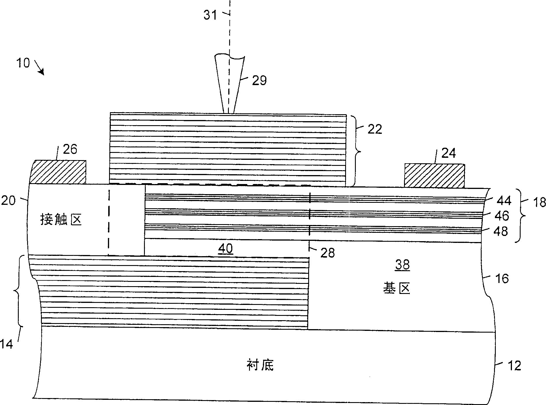
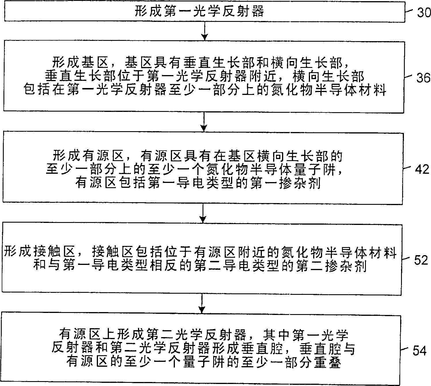
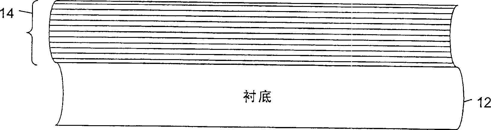
[0011] In the following description, similar reference numerals are used to designate similar elements. Moreover, the drawings are intended to show major configurations of exemplary embodiments in diagrammatic form. The drawings are not intended to depict every configuration of actual embodiments and the relative dimensions of the depicted elements are not drawn to scale.

[0012] As used herein, the term "nitride semiconductor material" refers to a nitrogen-containing Group III-IV semiconductor material. Exemplary nitride semiconductor materials include gallium nitride (GaN), indium gallium nitride (InGaN), indium nitride (InN), aluminum gallium nitride (AlGaN), aluminum nitride (AlN), aluminum indium gallium nitride ( AlInGaN), gallium arsenide nitride (GaAsN), indium gallium arsenide nitride (InGaAsN), aluminum gallium arsenide nitride (AlGaAsN), gallium phosphide nitride (GaPN), indium gallium phosphide nitride (InGaPN) and aluminum gallium phosphonitride compound (AlGaP...


PUM


Abstract

The invention discloses a vertical cavity surface-emitting laser (VCSEL). The VCSEL includes a base region that has a vertical growth part laterally adjacent a first optical reflector and a lateral growth part that includes nitride semiconductor material vertically over at least a portion of the first optical reflector. An active region has at least one nitride semiconductor quantum well vertically over at least a portion of the lateral growth part of the base region and includes a first dopant of a first electrical conductivity type. A contact region includes a nitride semiconductor material laterally adjacent the active region and a second dopant of a second electrical conductivity type opposite the first electrical conductivity type. A second optical reflector is vertically over the active region and forms with the first optical reflector a vertical optical cavity overlapping at least a portion of the at least one quantum well of the active region. A method of fabricating a VCSEL also is described.

Description

technical field [0001] The invention relates to a nitride semiconductor vertical cavity surface emitting laser. Background technique [0002] A VCSEL is a laser device formed from an optically active semiconductor region sandwiched between a pair of highly reflective mirror stacks, which may be formed from several layers of metallic material, dielectric material, or epitaxially grown semiconductor material. Recently, various efforts have been made to extend the operating wavelength of VCSEL devices to the shorter wavelength range of 200nm to 600nm (ie, the violet to red regions of the visible spectrum). Many nitride semiconductor materials (for example, GaN-based materials such as GaN, AlGaN, and AlInGaN) have bandgap energies corresponding to this wavelength range. For this reason, many efforts have been made to manufacture nitride semiconductor light emitting devices that generate light in this wavelength range. [0003] One of the issues related to designing high perfor...

Claims


Application Information

Patent Timeline
Patent Type & Authority Applications(China)
IPC IPC(8): H01S5/183H01S5/343H01S5/187
CPCH01S5/18383H01S5/18369H01S5/20H01S5/0424H01S2304/12H01S5/34333B82Y20/00H01S5/18341H01S5/183
Inventor 斯科特·W·科尔扎因戴维·P·保尔
Owner AVAGO TECH ECBU IP (SINGAPORE) PTE LTD
Why Eureka
Try Eureka