Method and system for manufacturing semiconductor, base and recording medium used therefor

A device manufacturing method and semiconductor technology, applied in semiconductor/solid-state device manufacturing, instruments, electrical components, etc., to achieve the effects of simplifying OPC, high precision, and reducing occupied area

Inactive Publication Date: 2007-03-21
PANASONIC CORP
View PDF2 Cites 15 Cited by
  • Summary
  • Abstract
  • Description
  • Claims
  • Application Information

AI Technical Summary

Problems solved by technology

[0015] However, in the above method, although the computational complexity required for correction can be reduced, the basic cell unit must be fixed, and the increase of the cell area of ​​the dummy wiring pattern cannot be avoided
Therefore, this situation becomes a big problem preventing miniaturization and higher integration of cells

Method used


Image

  • Method and system for manufacturing semiconductor, base and recording medium used therefor
  • Method and system for manufacturing semiconductor, base and recording medium used therefor
  • Method and system for manufacturing semiconductor, base and recording medium used therefor

Examples


Embodiment 1

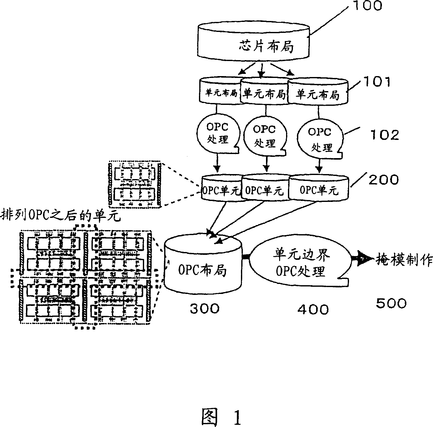
[0059] FIG. 1 is a view showing the concept of the semiconductor device manufacturing method of Embodiment 1 of the present invention.

[0060] As shown in FIG. 1, the method includes the steps of dividing the layout data of the integrated circuit constituting the semiconductor device into a plurality of units; applying the OPC step of optical proximity correction (hereinafter abbreviated as OPC) to each unit; Then, exposure is performed based on the layout data to form a desired pattern; a step of arranging / compositing each OPC-applied cell to which the OPC processing step is applied; and a step of correcting the boundary portion of the cell through the boundary area OPC processing.

[0061] In other words, as shown in the conceptual diagram of FIG. 1, the cell layout data 101 is generated by dividing the layout data 100 for each cell, and then, cell OPC processing is performed on each cell layout data (step 102). Therefore, the OPC unit 200 is obtained. Next, the OPC layout 300 ...

Embodiment 2

[0080] Next, Embodiment 2 of the present invention is explained below.

[0081]In the above example 1, select the border parts that frequently appear in the combination of adjacent unit arrangements, then remove the frequently occurring border part patterns, and then take out the border part patterns from the library and arrange them in the corresponding In this area, the correction accuracy can be improved. In this embodiment, simplified correction can be achieved by only reducing the pattern of the adjacent cell boundary area after the arrangement.

[0082] Fig. 5 shows a processing flow for explaining the method.

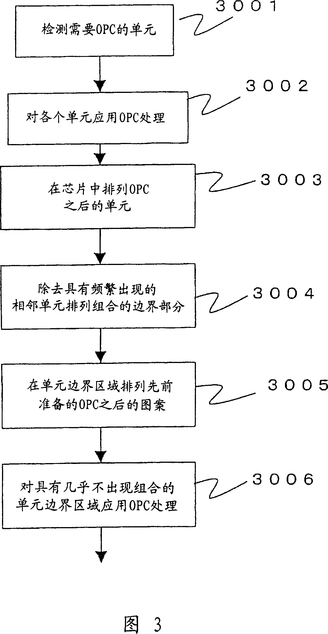
[0083] First, similar to Embodiment 1, from the layout data input by the layout data input section, a cell requiring OPC is selected at an appropriate level (step 5001). Next, OPC processing is applied to the selected units respectively (step 5002).

[0084] Next, based on the cell layout arrangement information before applying OPC, the cells after the OPC processed ...

Embodiment 3

[0092] Next, Embodiment 3 of the present invention is explained below.

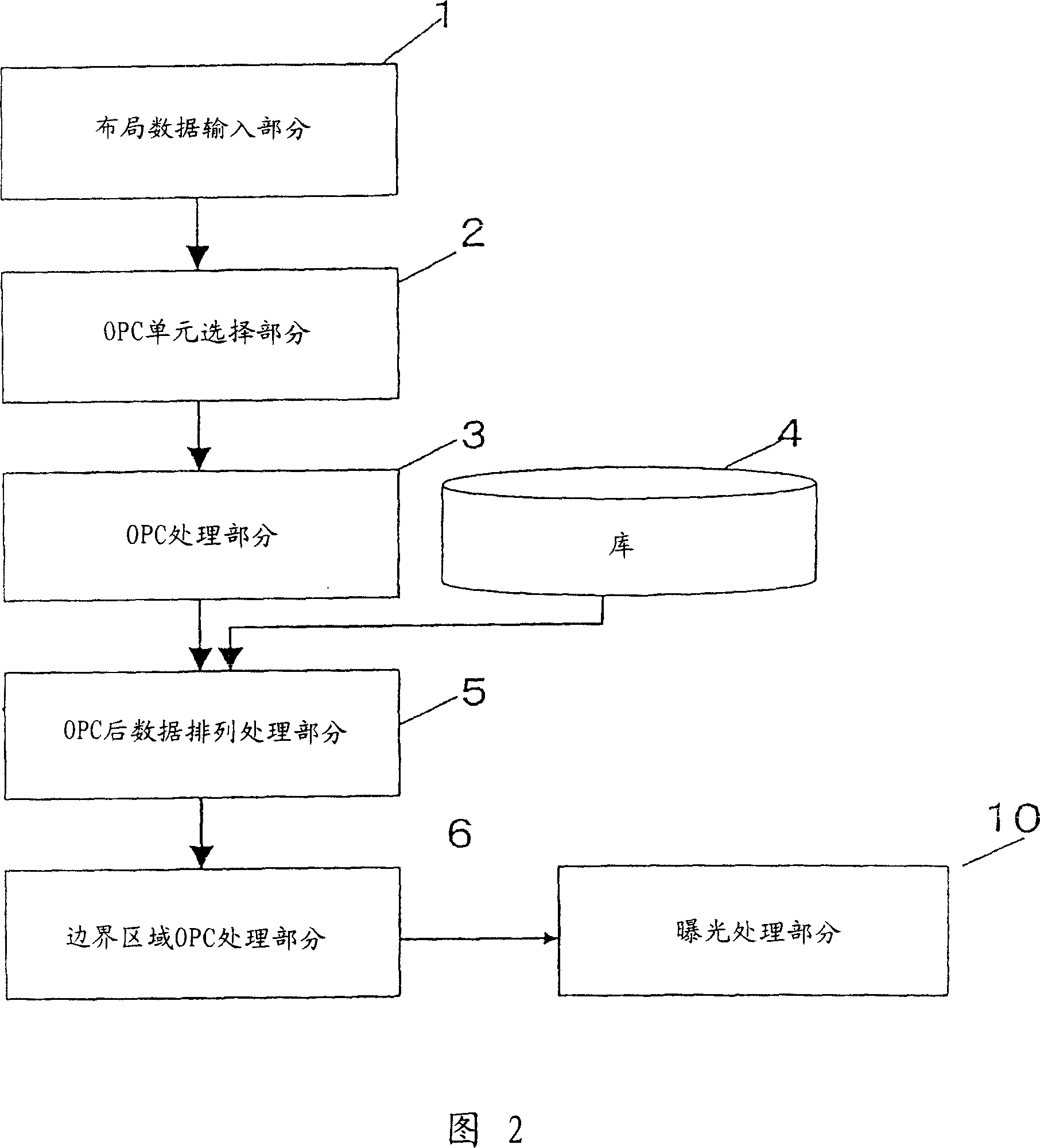
[0093] As shown in FIG. 6, the semiconductor device manufacturing system, in addition to the system shown in FIG. 2 and explained in Embodiment 1, also has a verification function part. The verification function part has: a library / block lithography verification selection part 7 for selecting a cell (block) to be verified from the layout data input by the layout data input part 1; a photolithography verification processing part 8 for The lithography verification is applied to the cell selected by the verification selection section 7; the boundary area photolithography verification processing section 9 is used to apply the lithography verification to the cell boundary area.

[0094] The lithography verification processing section 8 simulates the cells selected by the verification selection section 7 by using the output data of the OPC processing section 3, and then compares the simulation results with the corr...


PUM


Abstract

To provide a semiconductor device manufacturing method of making a pattern formation possible with high precision at a high speed, the same block can be completed by one process a cell by dividing the layout data into cells in the OPC processing step and then applying the OPC to each cell, and the OPC is applied only to the cell boundary portions after respective OPC-applied cells are arranged on the chip, so that a dimensional precision in vicinity of the cell boundaries can be ensured. Also, since the patterns on the cell boundary portions are caused to shrink uniformly, the OPC of the cell boundary portions can be simplified and thus the fast process can be applied.

Description

Technical field [0001] The present invention relates to a semiconductor device manufacturing method and a library, a recording medium and a semiconductor device manufacturing system used in the semiconductor device manufacturing system, in particular to the correction of design patterns to reduce the influence of the optical proximity effect in the semiconductor device design method, and also to pattern verification. Background technique [0002] In each step of the semiconductor R&D or development and trial production stages, computer simulation technology is currently used as an indispensable technology for semiconductor design as a technology for mastering processing or product characteristics that depend on manufacturing conditions, and prediction and evaluation of virtual test characteristics. . [0003] Specifically, simulation technology of photolithography processing used as fine pattern processing technology (the core of semiconductor manufacturing technology) is theoret...

Claims


Application Information

Patent Timeline
Patent Type & Authority Applications(China)
IPC IPC(8): G03F7/20H01L21/00G03F1/36G03F1/68H01L21/027
CPCG03F7/70441G03F7/70433
Inventor 神代昌彦谷本正
Owner PANASONIC CORP
Why Eureka
Try Eureka