
Patsnap Eureka
For R&D, Patsnap Eureka makes reading and utilizing patents & technical documents easy.
Patsnap Eureka AIR
Designed for self-driven R&D workflows. Generate viable solutions, solve complex R&D challenges, empower your innovation with AI.

Patsnap Eureka Materials
Designed for material experts only. Revolutionize your material R&D, from search, analyze, to developing new materials.

TechResearch
Generate reliable direction feasibility study reports for your R&D in just a few steps.

TechSeek
Discover and master advanced knowledge NOW. Basics, ideas, possibilities, all at once.

TechMind
As an expert in R&D Theories, TechMind can generates customized viable solutions instantly.

TechRisk
Analyze your overall solution with one click, know your potential R&D risks in advance.

TechMonitor
Get weekly tech updates, stay abreast of the latest tech innovations and key insights.
Vertical color filter sensor group and semiconductor integrated circuit fabrication method for fabricating same
A sensor group, sensor technology, applied in the direction of semiconductor devices, circuits, electrical components, etc., can solve the problems of non-standard manufacturing technology, inability to choose different color readout, and high sensor density
- Summary
- Abstract
- Description
- Claims
- Application Information
AI Technical Summary
Problems solved by technology
Method used
Image

Examples
Embodiment Construction
[0057] Those of ordinary skill in the art will appreciate that the following description of the invention is illustrative only and not restrictive in any way. Other embodiments of the invention will readily occur to those skilled in the art having the benefit of the invention.
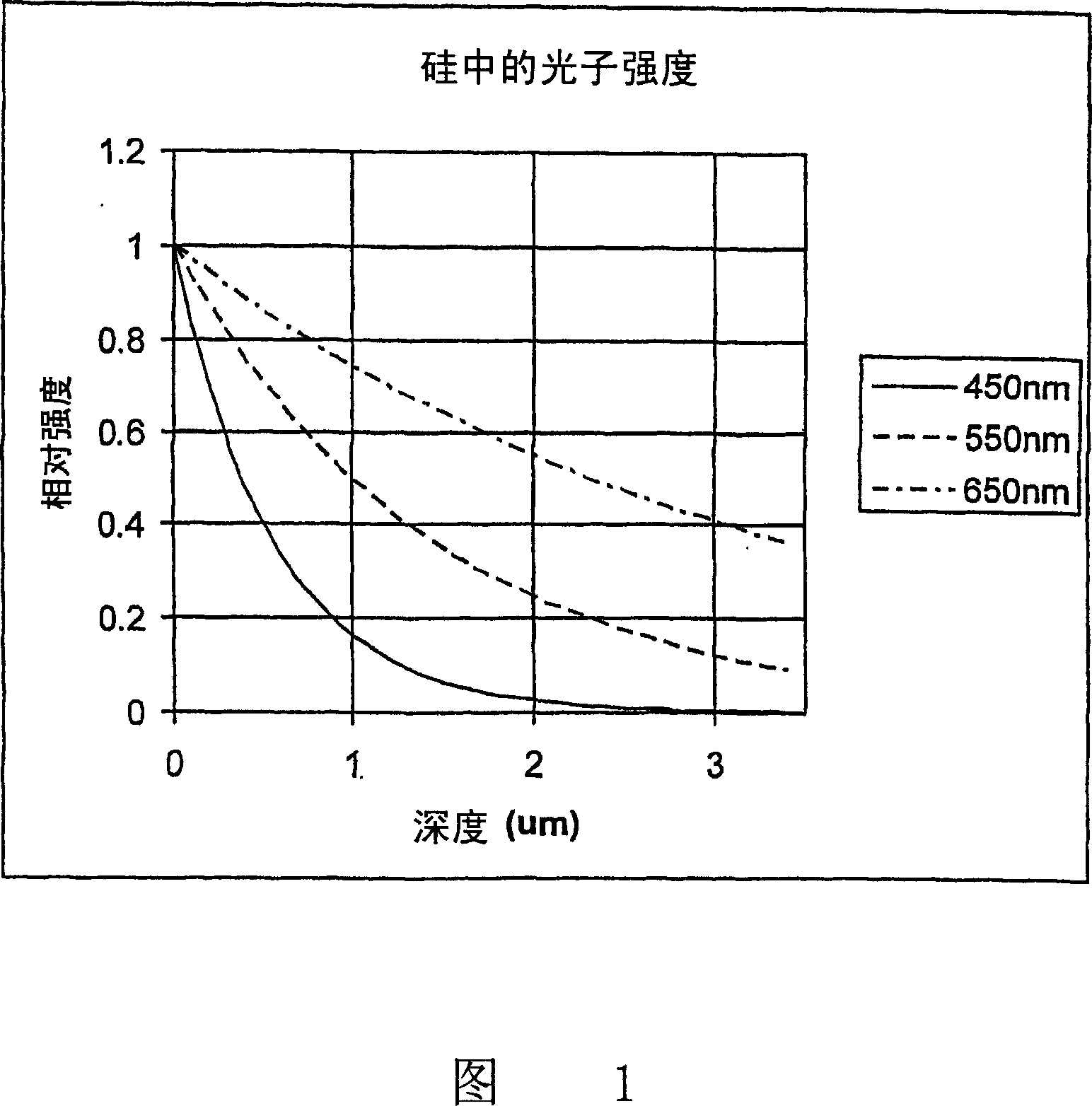
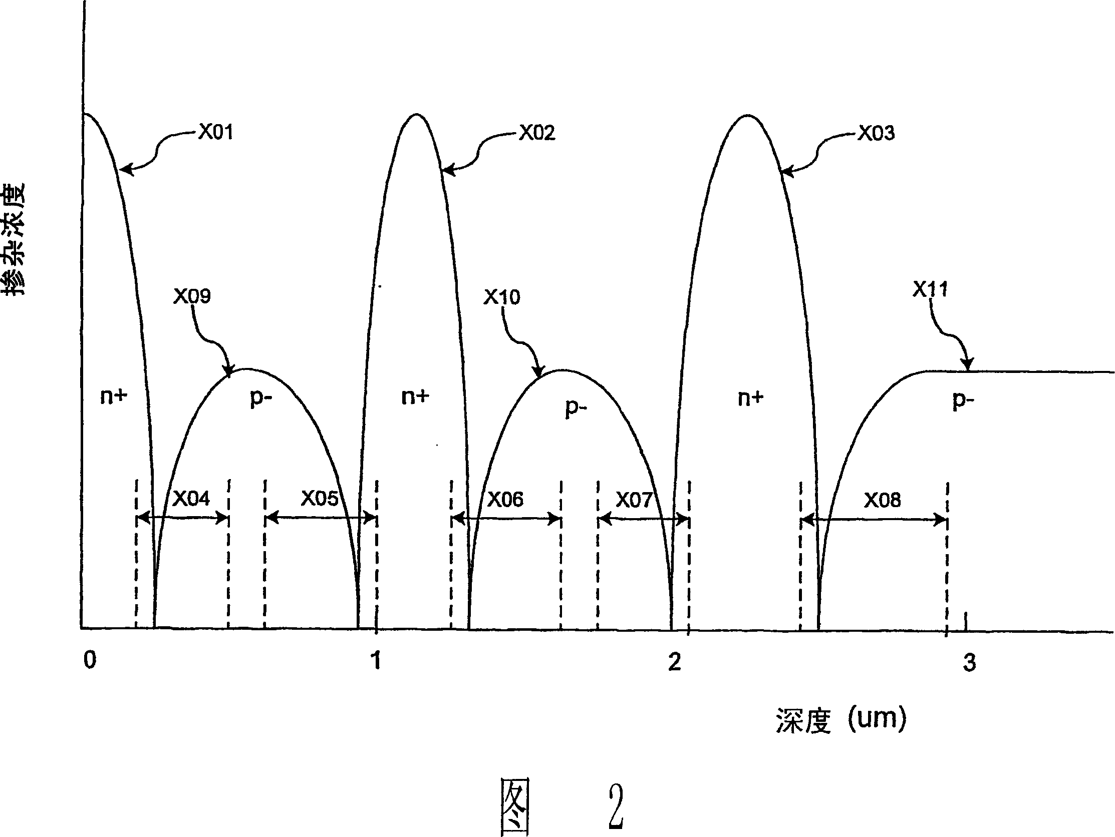
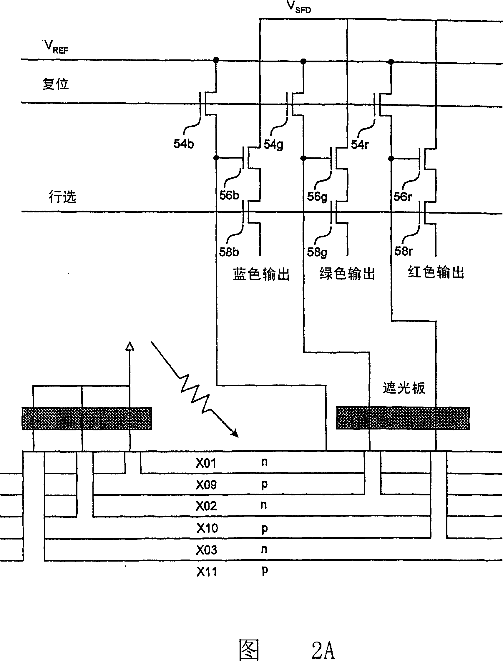
[0058] Most of the fabrication process to be described herein assumes that the sensor is made of crystalline silicon, but the method (or modifications to it that will be obvious to those skilled in the art) can generally be applied to sensors made of other semiconductor materials as well. . Each sensor of the VCF sensor group detects photons by directly or indirectly converting the energy of the photons into electron-hole pairs. This occurs in semiconducting materials. Groups of VCF sensors are typically implemented such that the output of each sensor in the group represents a different waveband of incident radiation. The radiation reaching each sensor in the VCF sensor group has a different wavelengt...
PUM
 Abstract
Description
Claims
Application Information
 - R&D Engineer
- R&D Manager
- IP Professional
- Industry Leading Data Capabilities
- Powerful AI technology
- Patent DNA Extraction
Browse by: Latest US Patents, China's latest patents, Technical Efficacy Thesaurus, Application Domain, Technology Topic, Popular Technical Reports.
© 2024 PatSnap. All rights reserved.Legal|Privacy policy|Modern Slavery Act Transparency Statement|Sitemap|About US| Contact US: help@patsnap.com