Femto-second laser ture three-D micro-nano-processing center

A femtosecond laser and micro-nano processing technology, applied in laser welding equipment, metal processing equipment, optics, etc., can solve limitations and other problems and achieve high-resolution effects

Inactive Publication Date: 2007-04-18
XI AN JIAOTONG UNIV
View PDF0 Cites 16 Cited by
  • Summary
  • Abstract
  • Description
  • Claims
  • Application Information

AI Technical Summary

Problems solved by technology

Based on the above characteristics, the application of femtosecond laser processing in micro-nano processing has great potential, but from the current reports, femtosecond laser surface etching processing is mainly used for simple structural features such as microholes and microgrooves. Although some research institutions try to apply it to three-dimensional structure processing, the actual results are limited to two-dimensional and semi-structural processing of rubber materials.

Method used


Image

  • Femto-second laser ture three-D micro-nano-processing center
  • Femto-second laser ture three-D micro-nano-processing center
  • Femto-second laser ture three-D micro-nano-processing center

Examples


Embodiment Construction

[0022] The content of the present invention will be described in detail below in conjunction with the accompanying drawings.

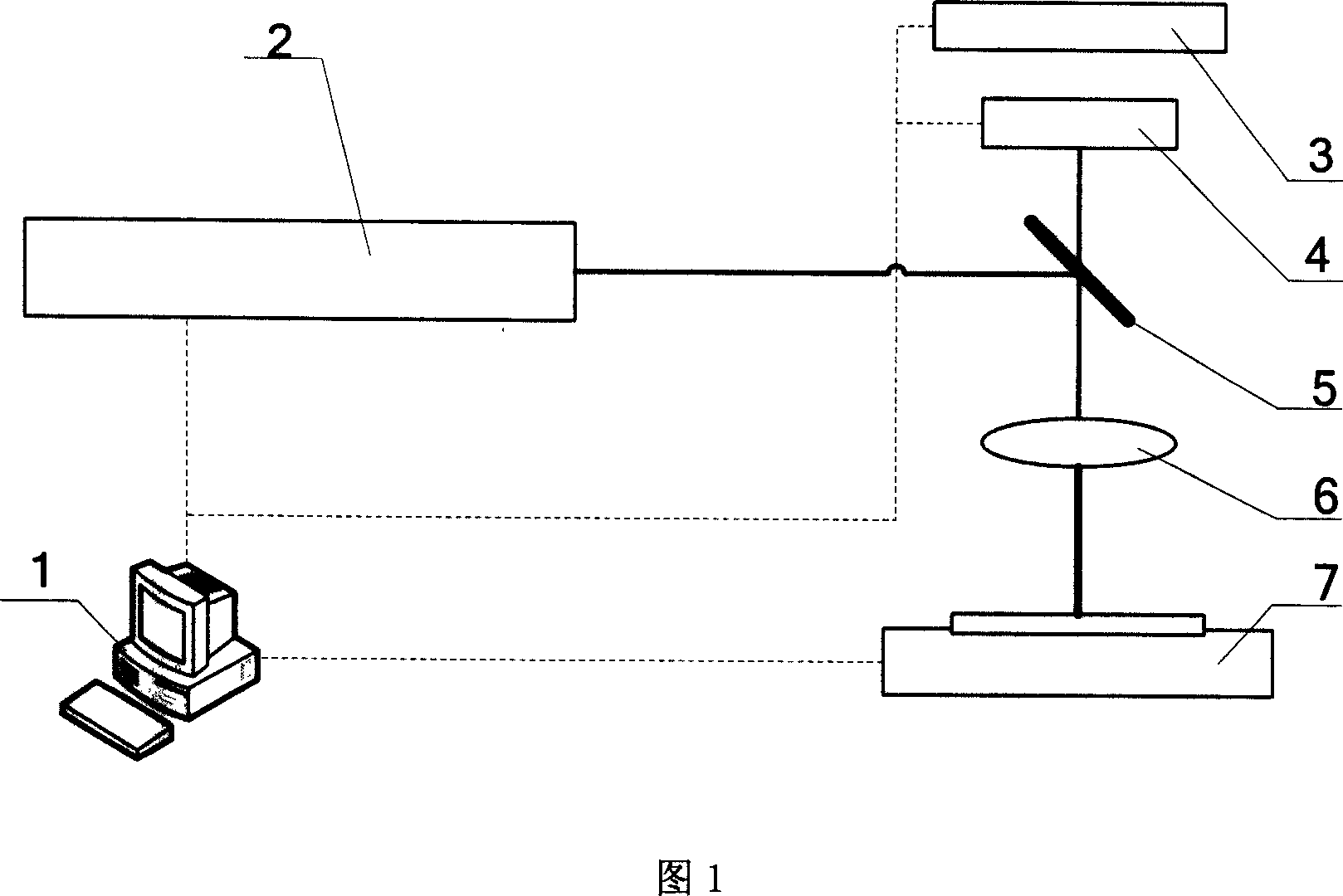
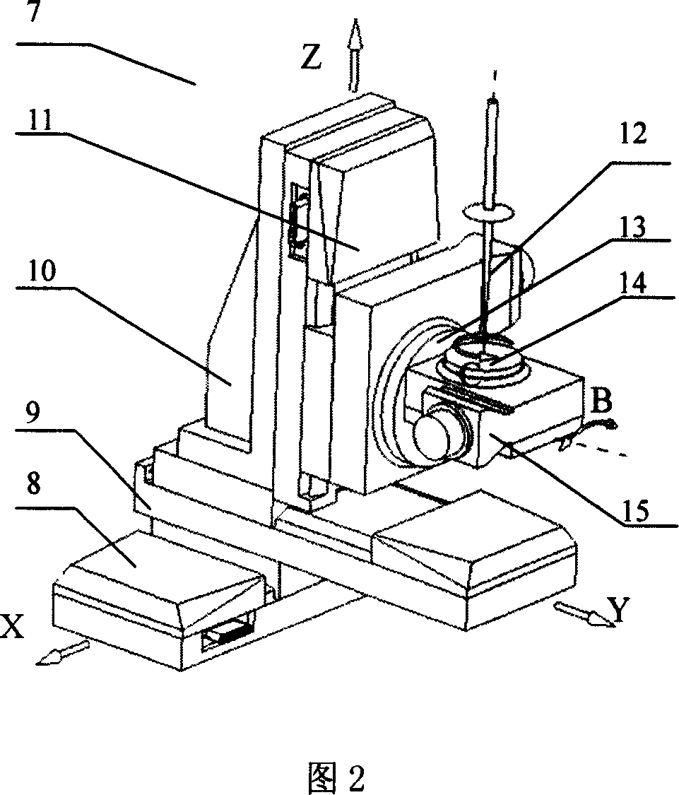
[0023] With reference to shown in Fig. 1, the present invention is provided with reflecting mirror 5 along the output beam direction of femtosecond laser generation amplifying system 2, and the negative included angle of reflecting mirror 5 and output beam is 45 °, along the optical axis direction after reflection in reflection A multi-axis linkage micro-motion workbench 7 is set under the mirror 5, a focusing lens 6 is set in the direction of the optical axis between the mirror 5 and the multi-axis linkage micro-motion workbench 7, and a CCD sensor 4 is set above the reflection mirror 5, femtosecond The laser generation and amplification system 2 , the multi-axis linkage micro-motion workbench 7 , the CCD sensor 4 and the LCD monitor 3 are connected to the industrial computer 1 .

[0024] Femtosecond laser generation amplification system 2, mirror 5 a...


PUM


Abstract

A true-3D fm-class machining center with fs laser is composed of a fs laser generating-amplifying system, a reflector arranged on the laser output path of said laser generating-amplifying system by negative 45-degree angle, a multiple axles linked microbench under said reflector, a focusing lens between said reflector and microbench, a CCD sensor above said reflector, a LCD monitor, and an industrial control computer.

Description

technical field [0001] The invention relates to a true three-dimensional micro-nano processing equipment, which belongs to the field of advanced manufacturing technology, in particular to a femtosecond laser true three-dimensional micro-nano processing center. Background technique [0002] In recent years, with the increasing demand for microsystems, the three-dimensional structure and the diversification of materials have become a hot issue in the field of micro-nano manufacturing. [0003] The traditional MEMS process mainly adopts the silicon micromachining process developed from the IC process, and processes the required structure through mask etching. This process is generally limited to two-dimensional processing. The LIGA technology developed in Germany in the 1980s broke through the limitations of silicon micromachining technology in the manufacture of high aspect ratio structures. At the same time, microdevices made of metal and plastic materials can also be produce...

Claims


Application Information

Patent Timeline
Patent Type & Authority Applications(China)
IPC IPC(8): B23K26/04B23K26/06B23K26/08B23K26/42G02B27/10B23K26/064B23K26/70
Inventor 赵万华薛飞李涤尘陈烽
Owner XI AN JIAOTONG UNIV
Why Eureka
Try Eureka