Crystal wafer testing method and structure of LED

A technology of light-emitting diodes and testing methods, which is applied in semiconductor/solid-state device testing/measurement, electrical components, electrical solid-state devices, etc., and can solve the problems of many manufacturing and testing machines, lengthy testing time, and low efficiency.

Active Publication Date: 2007-05-02
CHIPMOS TECH INC
View PDF0 Cites 6 Cited by
  • Summary
  • Abstract
  • Description
  • Claims
  • Application Information

AI Technical Summary

Problems solved by technology

The existing known manufacturing process of light-emitting diodes is to prepare an LED semiconductor wafer first, cut the wafer into LED chips, rearrange them on a belt-shaped conveyor belt, and use probes at both ends to contact the P of a single LED chip. Type electrodes and N-type electrodes, after testing whether they emit light, move the probe and test the next LED chip, so each LED chip is tested one by one, the test time is lengthy, and then each LED chip Individually placed on a substrate (or lead frame), electrically connect the LED chip and the substrate (or lead frame) by wire bonding, then seal the LED chip with a transparent resin or glass cover, and finally test the packaged LED chip again , its manufacturing process and testing require quite a variety of different handling types, resulting in too many manufacturing and testing machines, and the efficiency is not obvious
[0003] It can be seen that the above-mentioned existing test method and structure of light-emitting diodes obviously still have inconvenience and defects in test method, product structure and use, and need to be further improved urgently.
In order to solve the problems existing in the test method and structure of light-emitting diodes, the relevant manufacturers have tried their best to find a solution, but no suitable design has been developed for a long time, and the test method and structure of general light-emitting diodes are not suitable. All the test methods and structures can solve the above problems, which is obviously a problem that the relevant industry is eager to solve

Method used


Image

  • Crystal wafer testing method and structure of LED
  • Crystal wafer testing method and structure of LED
  • Crystal wafer testing method and structure of LED

Examples


Embodiment Construction

[0038] In order to further explain the technical means and effects of the present invention to achieve the intended purpose of the invention, the following in conjunction with the accompanying drawings and preferred embodiments, the specific implementation of the wafer-level testing method and structure of the light-emitting diode proposed according to the present invention, The test method, steps, structure, characteristics and efficacy are described in detail below.

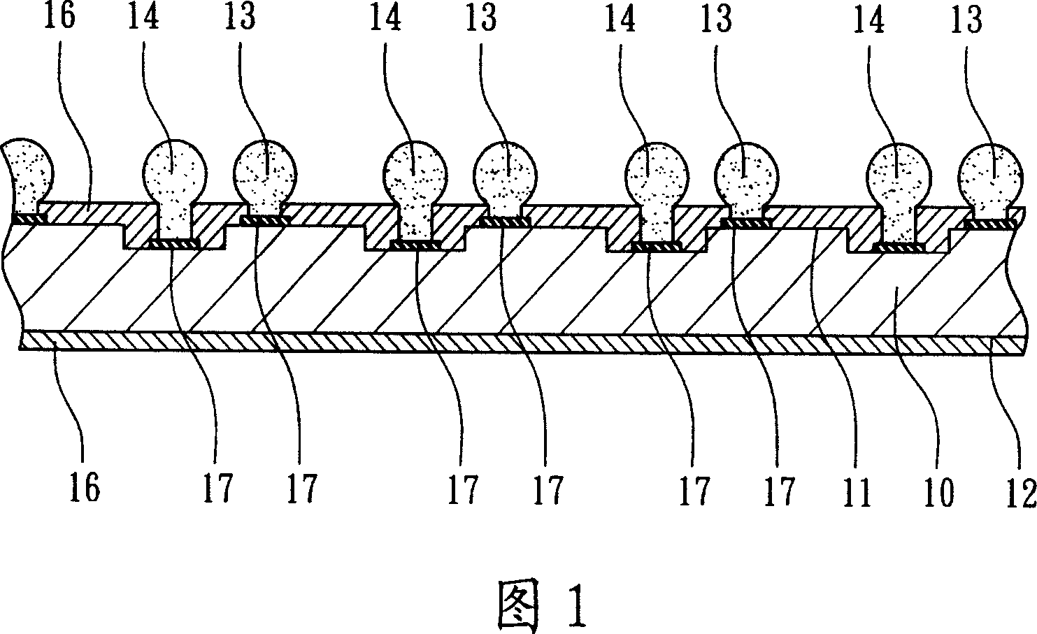
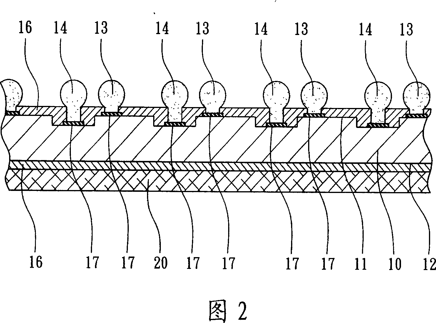
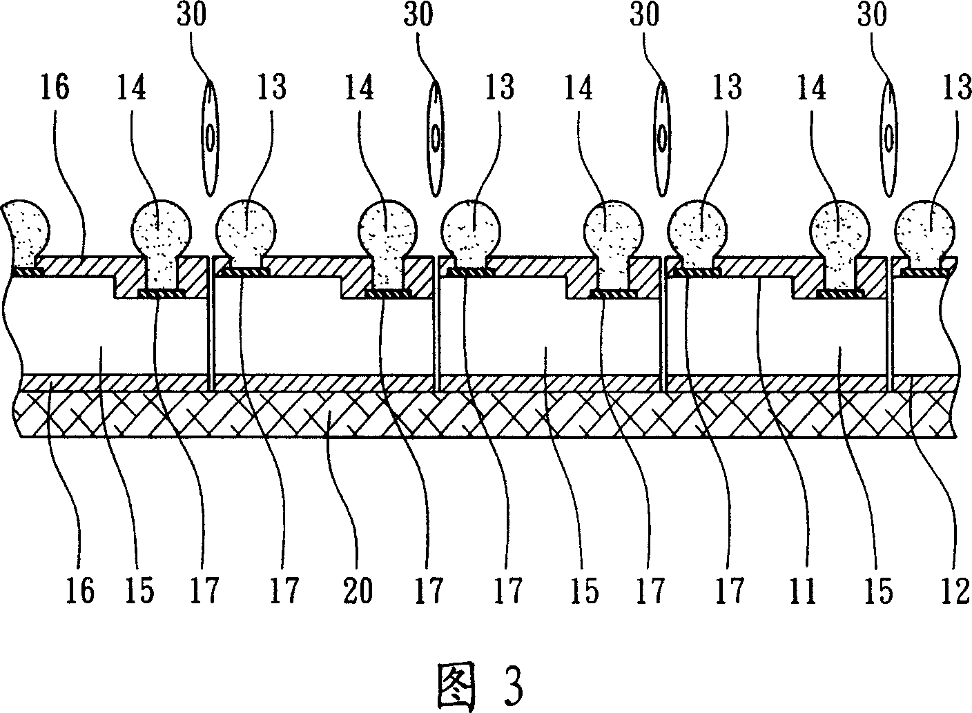
[0039] Please refer to FIG. 1 , which is a schematic cross-sectional view of an LED semiconductor wafer provided by the wafer-level testing method for light-emitting diodes according to the present invention. According to the wafer level test method of light emitting diode of the present invention, it mainly comprises the following steps: first, provide an LED semiconductor wafer 10 (LED is the abbreviation of Light Emitting Diode, or claim light emitting diode), this LED semiconductor wafer 10 Having a front s...


PUM


Abstract

A method for testing grade of chip on LED includes sticking an adhesive tape at back said chip, cutting it to be multiple LED chip with adhesive tape, contacting P type and N type of electrodes on those chips by detection card with multiple detection structures in ohm mode, setting a light detector on each of said detection structure, setting these light detector correspondingly above those chips and using them to detect light source emitted by those Led chips.

Description

technical field [0001] The invention relates to a testing method and structure of a light-emitting diode, in particular to a wafer-level testing method and structure of a light-emitting diode. Background technique [0002] The conventional Light Emitting Diode (LED) is composed of P-N junction semiconductors. When the current flows from the P side to the N side, it emits light immediately, and can convert electric energy into a light source with high efficiency. The existing known manufacturing process of light-emitting diodes is to prepare an LED semiconductor wafer first, cut the wafer into LED chips, rearrange them on a belt-shaped conveyor belt, and use probes at both ends to contact the P of a single LED chip. Type electrodes and N-type electrodes, after testing whether they emit light, move the probe and test the next LED chip, so each LED chip is tested one by one, the test time is lengthy, and then each LED chip Individually placed on a substrate (or lead frame), el...

Claims


Application Information

Patent Timeline
Patent Type & Authority Applications(China)
IPC IPC(8): H01L21/66H01L33/00H01L33/36H01L33/52
CPCH01L2224/14
Inventor 刘安鸿王永和赵永清李耀荣
Owner CHIPMOS TECH INC
Why Eureka
Try Eureka