Structure of TFT LCD array base plate and manufacturing method of the same

A technology of an array substrate and a manufacturing method, applied to the structure of a TFT LCD array substrate and its manufacturing field, can solve problems such as waste, and achieve the effects of protecting the environment, preventing dust, and reducing emissions

Active Publication Date: 2007-05-16
K TRONICS (SUZHOU) TECH CO LTD +1
View PDF0 Cites 38 Cited by
  • Summary
  • Abstract
  • Description
  • Claims
  • Application Information

AI Technical Summary

Problems solved by technology

Smashing unqualified products is undoubtedly a waste for glass substr

Method used


Image

  • Structure of TFT LCD array base plate and manufacturing method of the same
  • Structure of TFT LCD array base plate and manufacturing method of the same
  • Structure of TFT LCD array base plate and manufacturing method of the same

Examples


Embodiment 1

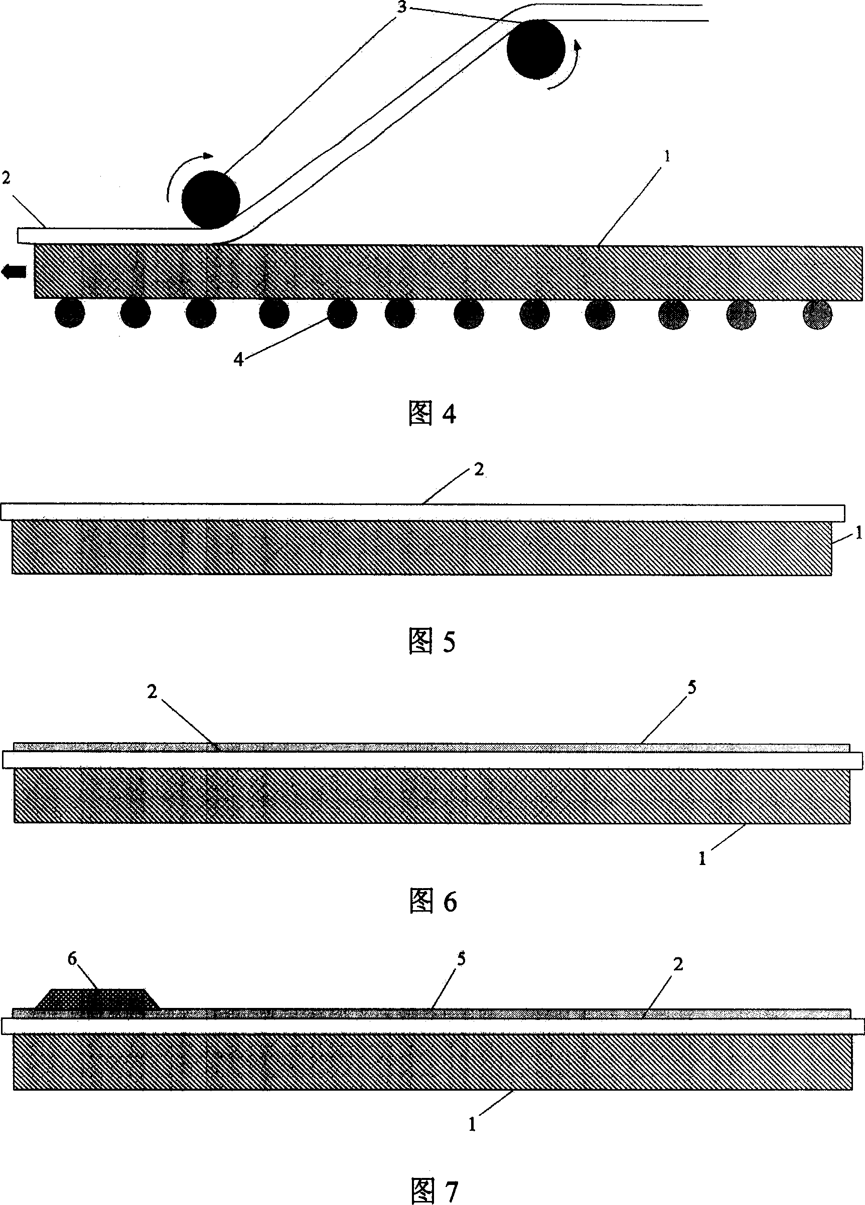
[0031] First of all, using a dedicated film laminating machine, relying on the film laminating roller 3 and atmospheric pressure on it, the polyimide film 2 is evenly pasted on the glass substrate 1 (the glass substrate 1 is placed on the glass substrate conveying roller 4). The method is shown in Figure 4. The specific structure of the cross-section after the polyimide film is pasted is shown in Figure 5. Some polyimide film products have an adhesive coated on one side to help them bond better to the glass substrate.

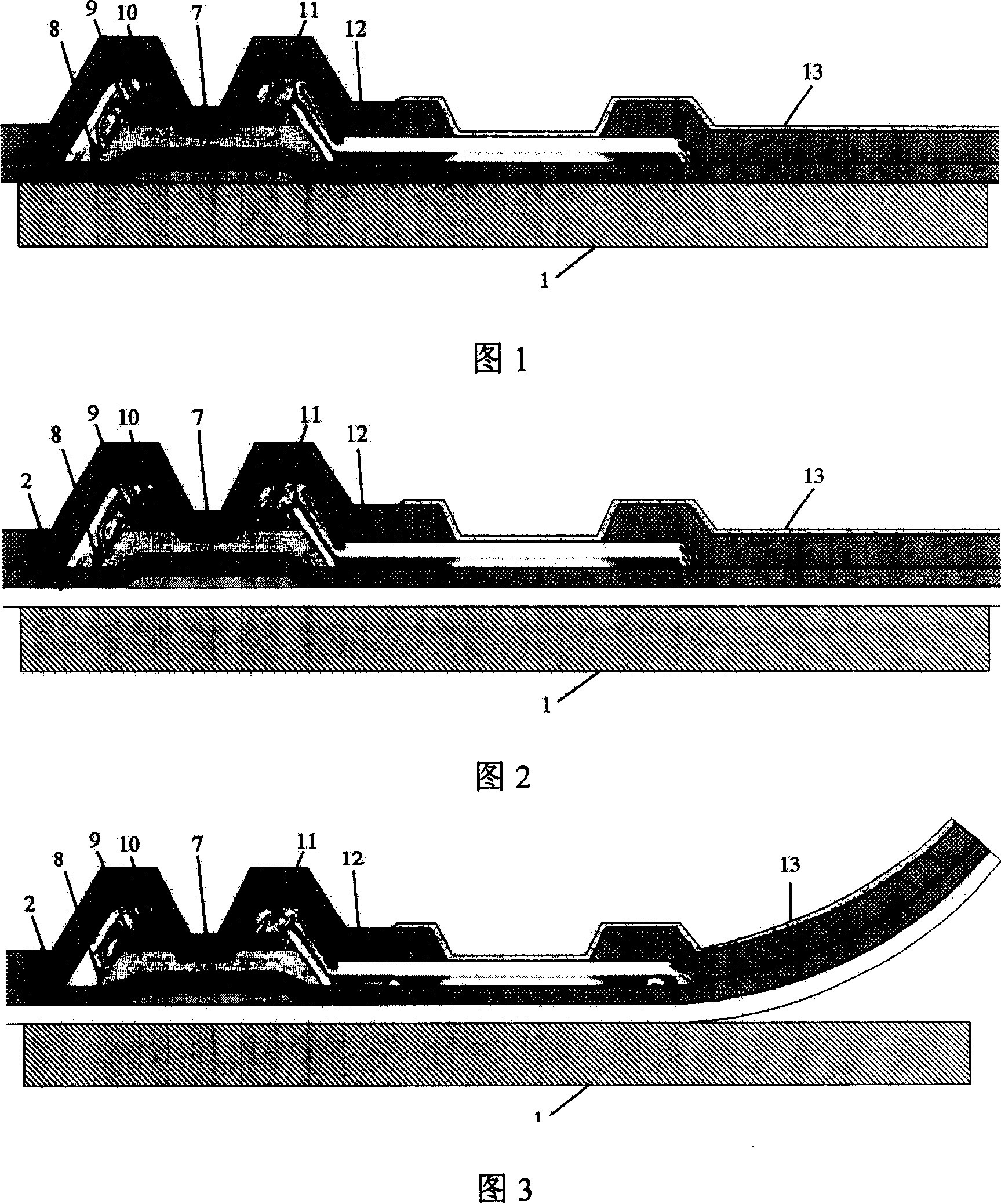
[0032] Then, a gate metal layer 5 is prepared on the polyimide film 2 by using methods such as sputtering, PECVD, MBE or printing, and its cross-sectional specific structure is shown in FIG. 6 . Then coat the photoresist on the film, and form the required pattern on the photoresist by mask exposure method, wherein the photoresist 6 of the gate part remains, and its cross-sectional specific structure is shown in FIG. 7 . The material area not protected by the ...

Embodiment 2

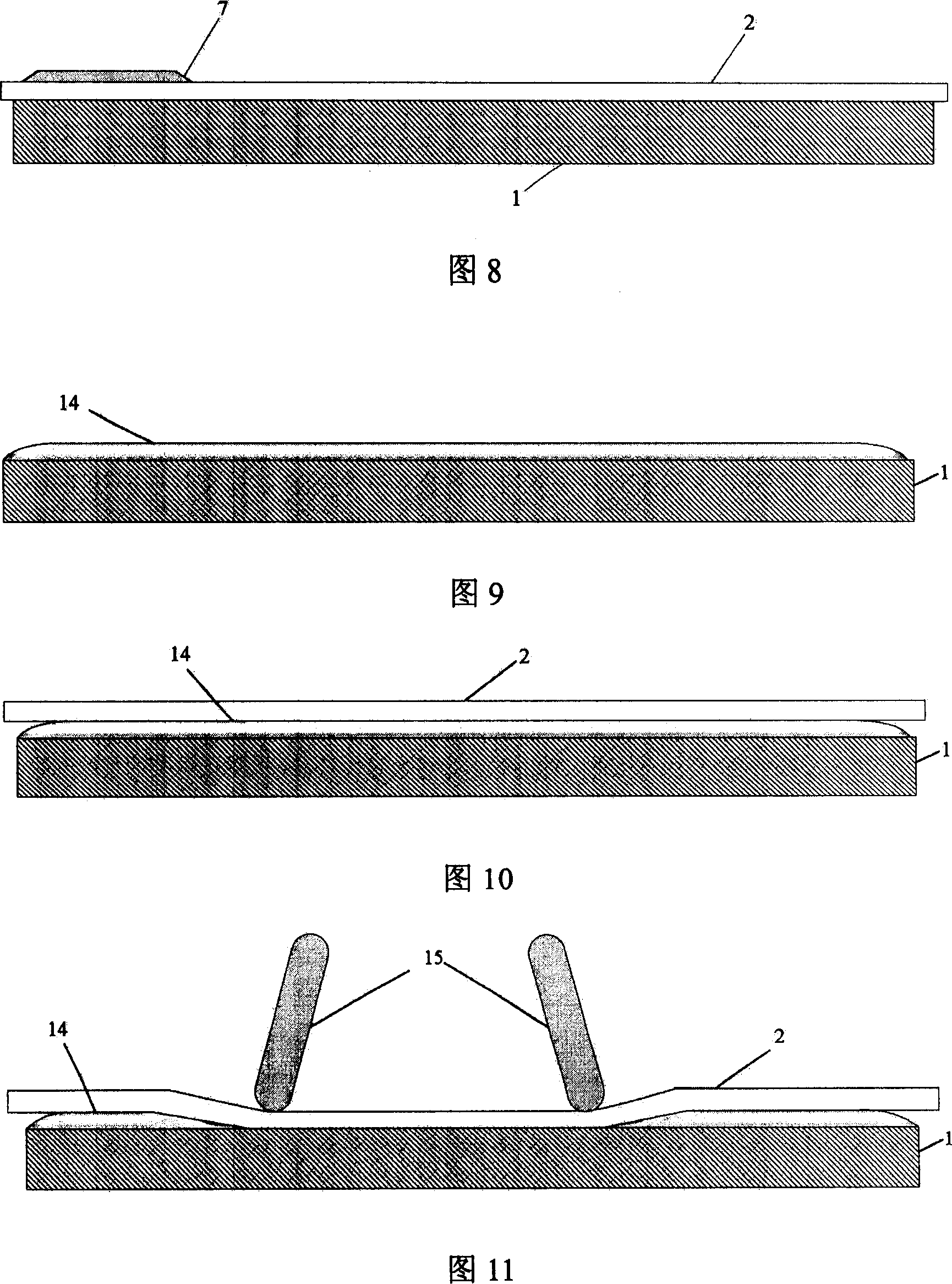
[0037] First, a layer of water film 14 is formed on the surface of the glass substrate by spraying or sprinkling, as shown in FIG. 9 . The function of the water film 14 is to improve the fluidity of the polyimide film, and remove the air bubbles retained on scratches, trachoma, pits and fabric depressions, thereby improving the flatness and uniformity of the film.

[0038]Then, a polyimide film with a size slightly larger than the glass substrate was placed on the glass substrate with the water film attached, as shown in Figure 10. After the film is positioned correctly, scrape it from the center to both sides with a rake-shaped plastic scraper 15 with a straight rubber end to remove internal air bubbles and moisture, as shown in Figure 11. If there is a local non-fitting place, heat it with a hair dryer to make the film and the glass completely bonded. After checking that there are no bubbles or wrinkles between the polyimide film and the glass substrate, prepare the require...


PUM


Abstract

This invention discloses one TFT LCD array base board structure, which comprises glass base board to form film transistor array on glass baseboard; one coating layer forming between glass base board and film transistor array with film layer as polyimide film. This invention also discloses one process method, which comprises the following steps: firstly providing one glass baseboard; then sticking polyimide film on glass baseboard; finally processing film transducer array on the polyimide film surface.

Description

technical field [0001] The invention relates to a structure of a thin film transistor liquid crystal display (TFT LCD) and a manufacturing method thereof, in particular to a structure of a TFT LCD array substrate and a manufacturing method thereof. Background technique [0002] Liquid crystal display (LCD) technology has developed rapidly in the past ten years, and great progress has been made in terms of screen size and display quality. After continuous efforts, the performance of all aspects of LCD has reached the level of traditional CRT, and there is a tendency to replace CRT. [0003] With the continuous expansion of LCD production, the competition among various manufacturers is becoming increasingly fierce. While continuously improving product performance, manufacturers are also making continuous efforts to reduce product production costs, thereby enhancing market competitiveness. In the cost of LCD display products, glass substrates occupy a large proportion. In th...

Claims


Application Information

Patent Timeline
IPC IPC(8): G02F1/1362G02F1/133
Inventor 周伟峰
Owner K TRONICS (SUZHOU) TECH CO LTD
Why Eureka
Try Eureka