

A porous silicon chip and its preparing method
A technology of porous silicon layer and silicon wafer, which is applied in the fields of semiconductor/solid-state device manufacturing, semiconductor/solid-state device components, semiconductor devices, etc. Problems such as harmful stress on the substrate, to achieve the effect of improving the resistivity of the substrate, widely used in the market, and low cost
- Summary
- Abstract
- Description
- Claims
- Application Information
AI Technical Summary
Problems solved by technology
Method used
Image

Examples
Embodiment 1
[0028] Embodiment 1, the preparation of back-facing thick-film porous silicon chip (SOP)
[0029] 1. Silicon wafer preparation: p-type bare silicon wafer, resistivity 12Ω cm, thickness 200μm
[0030] 2. Preparation of porous silicon:
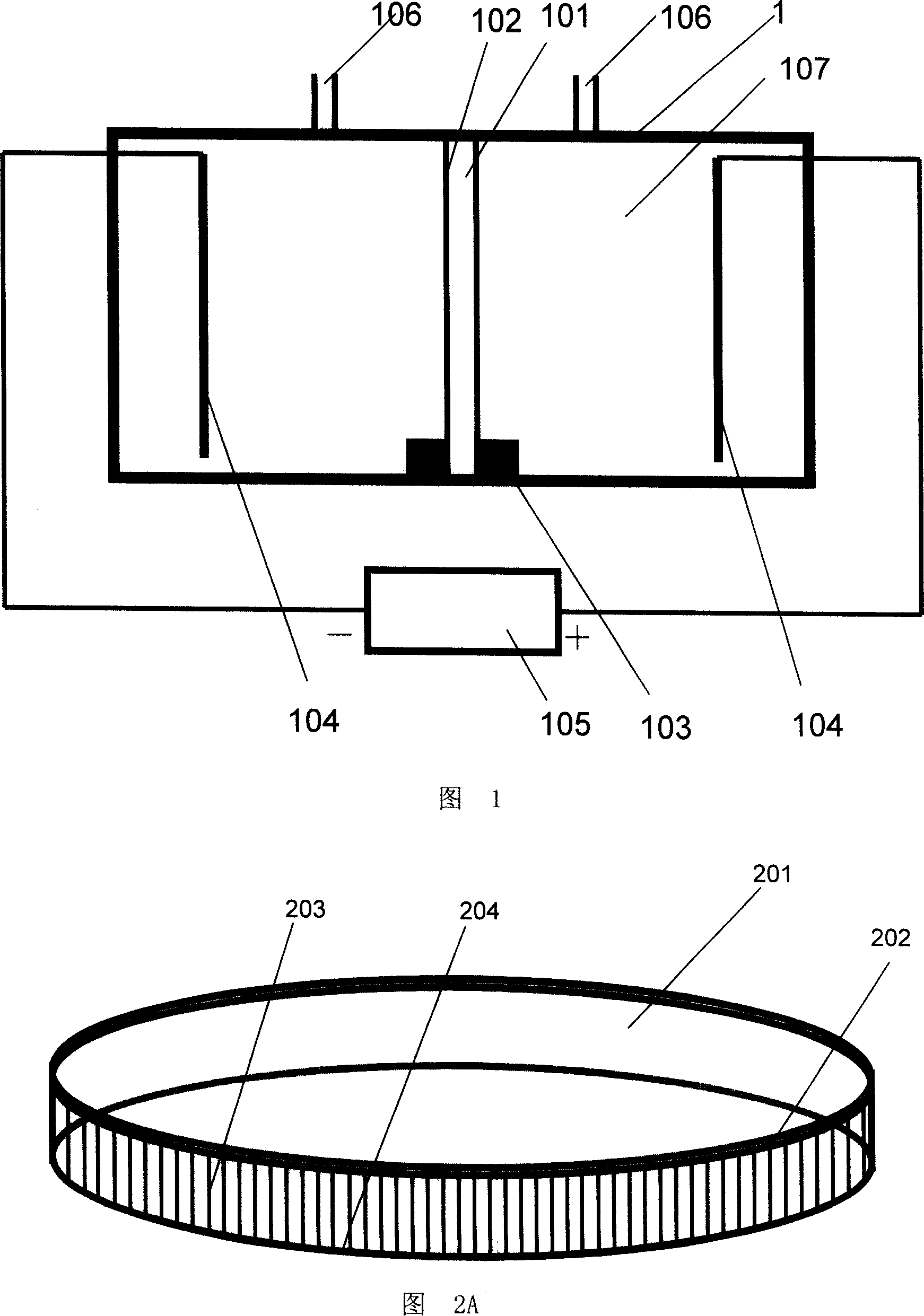
[0031] As shown in Figure 1, the used etching device comprises etching tank 1, has etching solution inlet 106 on it, and etching solution 107 is positioned at the inside of etching tank 1; In the corrosion tank 1 ; the precision constant current power supply 105 is connected with two platinum Pt electrodes 104 for supplying electric current. After electrification, the back side 102 of the silicon wafer on the cathode side of the silicon wafer will be corroded to form a porous silicon layer on the silicon wafer.
[0032] The ratio of the corrosion solution used: HF: DMF (volume ratio) = 1:4
[0033] Current density: 30mA / cm 2
[0034] Corrosion time: 135-140 minutes
[0035] After the above treatment, a porous silicon layer was formed on th...
Embodiment 2
[0047] Implementation Example 2 Preparation of back-facing thick-film porous silicon wafer (SOP)
[0048] 1. Silicon wafer preparation: p-type bare silicon wafer, resistivity 25Ω·cm, thickness 150μm
[0049] 2. Preparation of porous silicon:
[0050] Used device is identical with embodiment 1, and concrete operation condition is as follows:
[0051] Corrosion solution ratio: HF:DMF=1:10
[0052] Current density: 50mA / cm 2
[0053] Corrosion time: 125-128 minutes.
[0054] After the above treatment, a porous silicon layer was formed on the silicon wafer with a thickness of 148 μm; the thickness of the remaining silicon layer was 2 μm.
Embodiment 3
[0055] Implementation Example 3 Preparation of Backward Thick Film Porous Silicon Wafer (SOP)
[0056] 1. Silicon wafer preparation: p-type bare silicon wafer, resistivity 3Ω·cm, thickness 500μm
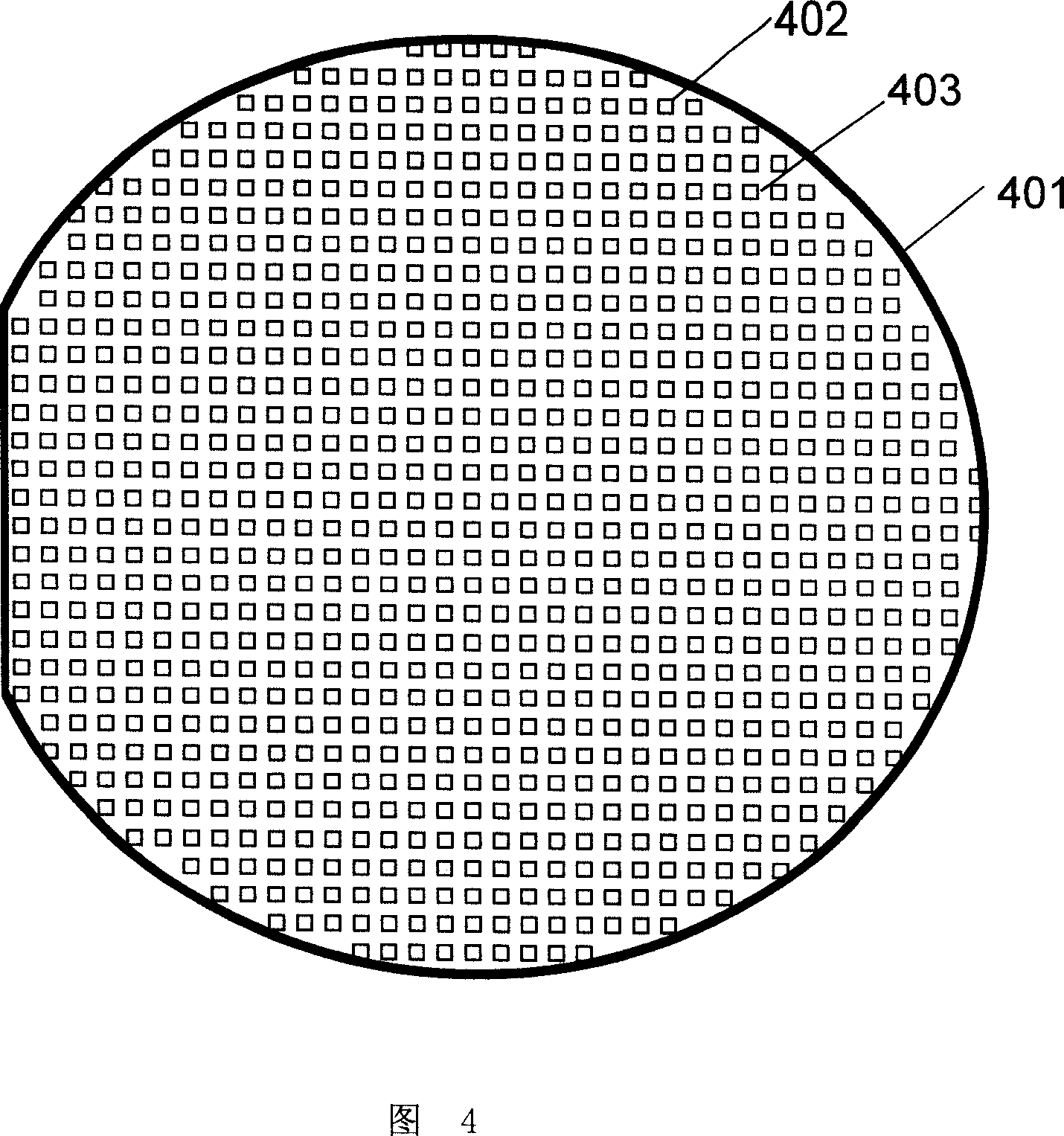
[0057] In order to increase the uniformity of the porous silicon etching area and the mechanical strength of the silicon wafer, a layer of Si is first deposited on the back of the silicon wafer. 3 N 4 A series of holes are formed by photolithography and etching: the diameter of the holes is 100 μm, and the gap between the holes is 10 μm.
[0058] As shown in Figure 4, a layer of Si is deposited on the backside 401 of the silicon wafer to be grown porous silicon layer 3 N 4 A series of square holes 402 are formed by photolithography and etching, and pores 403 are formed. Since Si 3 N 4 It ensures that its covered area is not corroded by the solution, so that the subsequent porous silicon is limited to Si 3 N 4 The series of close-packed hole regions opened by the layer are gen...
PUM
| Property | Measurement | Unit |
|---|---|---|
| Resistivity | aaaaa | aaaaa |
| Thickness | aaaaa | aaaaa |
| Resistivity | aaaaa | aaaaa |
Abstract
Description
Claims
Application Information