Si-based AlGaN/GaN high-electron-mobility transistor with wrapping buried layer and preparation method

A technology with high electron mobility and transistors, applied in transistors, semiconductor/solid-state device manufacturing, circuits, etc., can solve the problems of increasing radio frequency loss, lower substrate resistivity, and large radio frequency loss, so as to reduce radio frequency loss and improve substrate Effect of bottom resistivity

Pending Publication Date: 2022-01-14
XIDIAN UNIV
View PDF0 Cites 0 Cited by
  • Summary
  • Abstract
  • Description
  • Claims
  • Application Information

AI Technical Summary

Problems solved by technology

However, the radio frequency loss of silicon-based AlGaN / GaN HEMT is relatively large. One source of radio frequency loss is caused by the P-type conductive channel formed by Al diffusion into the silicon substrate. This conductive channel will increase additional radio frequency loss and make the substrate The resistivity of the bottom is reduced, and the RF loss is increased

Method used


Image

  • Si-based AlGaN/GaN high-electron-mobility transistor with wrapping buried layer and preparation method
  • Si-based AlGaN/GaN high-electron-mobility transistor with wrapping buried layer and preparation method
  • Si-based AlGaN/GaN high-electron-mobility transistor with wrapping buried layer and preparation method

Examples


Embodiment 1

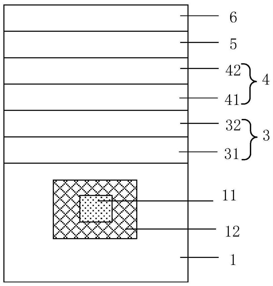
[0029] See figure 1 , figure 1 A structural diagram of a Si-based AlGaN / GaN high electron mobility transistor having a wrapped embedded layer is provided for an embodiment of the present invention.

[0030] The AlGaN / GaN high electron mobility transistor includes a Si substrate 1, AlN-ring-based 3, AlGa-step becomings 4, a GaN buffer layer 5, and a AlGa barrier layer 6, wherein the Si substrate 1 is provided in the Si substrate 1. The n-type buried layer 11 and the isolation layer 12 are disposed between the Si substrate 1 and the n-type buried layer 11 and wrap the N-type buried layer.

[0031] In this embodiment, the n-type buried layer 11 and the spacer layer 12 are each disposed in the Si substrate 1, i.e., the spacer layer 12 is wrapped in the four weeks of the n-type buried layer 11, and the Si substrate 1 is wrapped around the spacer 12. The arrangement of the isolation layer 12 satisfies the following conditions: The isolation layer 12 does not cover the n-type impurit...

Embodiment 2

[0053] On the basis of the first example, see Figure 3A-Figure 3F , Figure 3A-Figure 3F A process diagram of a method of preparing a Si-based AlGaN high electron mobility transistor having a wrap-embedding layer, wherein the preparation method comprises the step of:

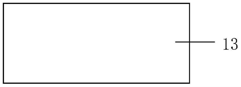
[0054] S1, prepare the first isolation sublayer 121 in the Si sheet 13, see Figure 3A and Figure 3B .

[0055] First, the Si sheet 13 is placed in a 20% HF acid solution soaking 60s, and then h 2 O 2 , Alcohol and acetone cleaning, and finally rinse 60s using flowing deionized water.

[0056] Then, the cleaned substrate was placed in a low pressure MoCVD reaction chamber, and hydrogen gas was passed, the temperature was raised to 950-1010 ° C, and the reaction chamber pressure was controlled to 40 torr, and the substrate was heat for 3 min under a hydrogen atmosphere.

[0057] Next, after the heat cleaning phase, the reaction chamber temperature is lowered to room temperature, and the Si sheet 13 is taken out, and th...

Embodiment 3

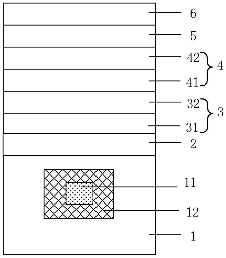
[0090] Based on the second embodiment, please figure 2 In this embodiment, another method of preparing another Si-based AlGaN high electron mobility transistor with a wrap layer, the preparation method comprising the step of:

[0091] S1, the first isolation sublayer 121 is prepared in the Si sheet 13.

[0092] S2, ionically implantation of the surface layer of the first isolation sublayer 121, forming the n-type buried layer 11.

[0093] S3, the second isolation sublayer 122 is grown on the first spacer layer 121 and the n-type buried layer 11 to form the isolation layer 12.

[0094] S4, a single crystal silicon 14 is grown on the Si sheet 13 and the second spacer 122 to form a Si substrate 1.

[0095] S5, preparing a pre-paved aluminum layer 2 on the Si substrate 1.

[0096] Specifically, the reaction chamber temperature is raised to 1080-1090 ° C, the TMAL air train is opened, and the TMAL flow rate is 10-30 Sccm, the preparation of the pre-pavomate layer 2 is performed, and th...


PUM

PropertyMeasurementUnit
Thicknessaaaaaaaaaa
Thicknessaaaaaaaaaa
Thicknessaaaaaaaaaa

Abstract

The invention relates to a Si-based AlGaN / GaN high electron mobility transistor with a wrapping buried layer and a preparation method. The high electron mobility transistor comprises a Si substrate, an AlN nucleating layer, an AlGaN order change layer, a GaN buffer layer and an AlGaN barrier layer which are stacked in sequence, an N-type buried layer and an isolation layer are arranged in the Si substrate, and the isolation layer is arranged between the Si substrate and the N-type buried layer and wraps the N-type buried layer. According to the high-electron-mobility transistor, the N-type buried layer and the isolation layer are arranged in the Si substrate, the isolation layer cannot completely mask N-type impurities in the N-type buried layer, and the N-type impurities can be diffused into the Si substrate so that the P-type channel concentration of the Si substrate introduced by Al diffusion in an upper-layer structure is counteracted, the resistivity of the substrate is improved, and the radio frequency loss of a device is reduced.

Description

Technical field [0001] The present invention is a semiconductor, and more particularly to a Si-based AlGaN / GaN high electron mobility transistor and a preparation method with a wrap-embedding layer. Background technique [0002] GaN is a typical representative of the third-generation wide-band semiconductor material. Because of its large ban, it is widely used in RF devices, LEDs and Power electronics. High Electron Mobility Transdomor, HEMT as a common GaN structure, is widely used in emerging 5G communication, radar and Space exploration and other areas, but this also puts a high demand for RF performance of the AlGan / GaN Hemt device. [0003] Conventional AlgaN / Gan Hent heterogeneous substrate is made of SiC, sapphire and Si substrate. Although SiC performance is best, due to the large size substrate is more expensive, it limits its large-scale commercial application; while sapphire substrates are limited because of poor thermal conductivity. Compared to the Si's substra...

Claims


Application Information

Patent Timeline
IPC IPC(8): H01L29/778H01L29/10H01L21/335
CPCH01L29/7786H01L29/1075H01L29/66462
Inventor 张雅超马金榜李一帆姚一昕张进成马佩军马晓华郝跃
Owner XIDIAN UNIV
Why Eureka
Try Eureka