Si-based GaN millimeter wave transmission line structure and preparation method
A technology of transmission line structure and millimeter wave, which is applied in the direction of waveguide, waveguide-type devices, electrical components, etc., and can solve the problems of complex preparation process, high transmission line loss, and insufficient to meet the application requirements of millimeter wave circuits.
- Summary
- Abstract
- Description
- Claims
- Application Information
AI Technical Summary
Problems solved by technology
Method used
Image

Examples
Embodiment 1
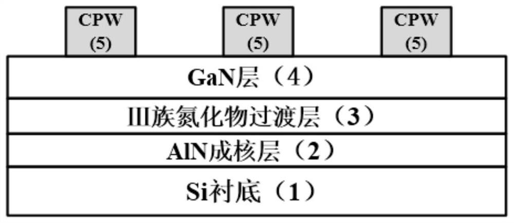
[0048] See Figure 4 , Figure 4 It is a structural schematic diagram of a Si-based GaN millimeter wave transmission line structure provided by an embodiment of the present invention. This embodiment provides a millimeter wave transmission line structure, and the preparation method of the millimeter wave transmission line structure includes:
[0049] Si substrate 10;
[0050] AlN nucleation layer 20, located on the Si substrate 10;
[0051] III-nitride transition layer 30, located on the AlN nucleation layer 20;
[0052] a GaN layer 40 located on the III-nitride transition layer 30;
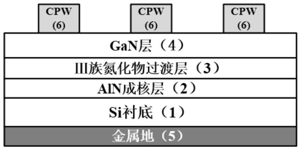
[0053] a metal ground 50 located on the GaN layer 40;
[0054] a dielectric insertion layer 60 with several through holes, located on the metal ground 50;
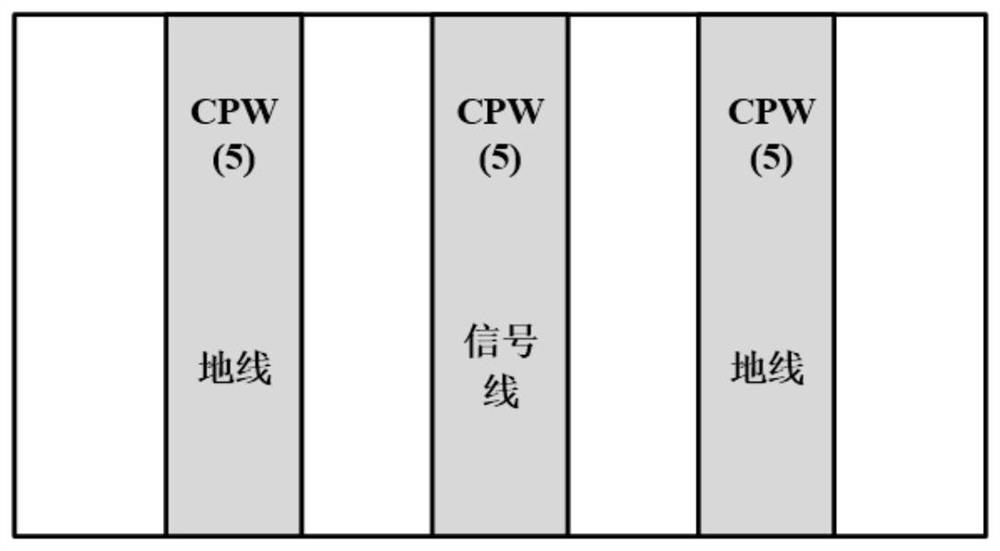
[0055] Several CPWs 80 are located on the dielectric insertion layer 60 , and each CPW 80 is correspondingly connected to the metal ground 50 through a through hole.
[0056]Further, the material of the metal ground 50 may include Au, ...
Embodiment 2
[0061] See Figure 5 , Figure 6a-Figure 6h , Figure 5 is a schematic flowchart of a method for preparing a millimeter wave transmission line structure provided by an embodiment of the present invention, Figure 6a-Figure 6h It is a structural schematic diagram of a millimeter wave transmission line structure provided by an embodiment of the present invention. This embodiment provides a method for preparing a millimeter-wave transmission line structure, and the method for preparing the millimeter-wave transmission line structure includes:
[0062] Step 1, such as Figure 6a As shown, the Si substrate 10 is selected.
[0063] Step 2, such as Figure 6b As shown, an AlN nucleation layer 20 is prepared on a Si substrate 10 .
[0064] Specifically, the AlN nucleation layer 20 is prepared on the Si substrate 10 by MOCVD (Metal-organic Chemical Vapor Deposition, metal-organic compound chemical vapor deposition).
[0065] Step 3, if Figure 6c As shown, a III-nitride transit...
Embodiment 3
[0087] In this embodiment, the Si substrate 10, the AlN nucleation layer 20, the III-nitride transition layer 30, and the GaN layer 40 are sequentially prepared from bottom to top in accordance with the method of the first embodiment. The rest of the steps are described in a specific implementation manner. After the Si substrate 10, the AlN nucleation layer 20, the III-nitride transition layer 30 and the GaN layer 40 are prepared, the following steps can also be specifically performed:
[0088] S1: cleaning the Si-based GaN structure, that is, cleaning the Si substrate 10 , the AlN nucleation layer 20 , the III-nitride transition layer 30 and the GaN layer 40 arranged sequentially from bottom to top.
[0089] Specifically, the Si substrate 10, AlN nucleation layer 20, III-nitride transition layer 30, and GaN layer 40 prepared from bottom to top were ultrasonically cleaned with acetone, isopropanone, and deionized water for 5 min in sequence, and then cleaned with High-purity n...
PUM
| Property | Measurement | Unit |
|---|---|---|
| thickness | aaaaa | aaaaa |
| thickness | aaaaa | aaaaa |
Abstract
Description
Claims
Application Information
 - R&D
- Intellectual Property
- Life Sciences
- Materials
- Tech Scout
- Unparalleled Data Quality
- Higher Quality Content
- 60% Fewer Hallucinations
Browse by: Latest US Patents, China's latest patents, Technical Efficacy Thesaurus, Application Domain, Technology Topic, Popular Technical Reports.
© 2025 PatSnap. All rights reserved.Legal|Privacy policy|Modern Slavery Act Transparency Statement|Sitemap|About US| Contact US: help@patsnap.com