An ultra-low loss device of drain-source region dielectric/pn junction isolation front gate p/n-mosfet radio frequency switch based on soi process

A technology of front gate and source region, applied in semiconductor devices, electrical components, transistors, etc., can solve problems such as being unfavorable to improve the overall performance of devices and systems, large losses, and low device efficiency.

Active Publication Date: 2016-08-24
HANGZHOU DIANZI UNIV
View PDF4 Cites 0 Cited by
  • Summary
  • Abstract
  • Description
  • Claims
  • Application Information

AI Technical Summary

Problems solved by technology

When the SOI P(N)-MOSFET device works normally, the channel formed by the conduction of source and drain is only on the top surface of the N(P)-type channel region, and it is a lateral channel, and the gate field plate covers the gate oxide layer, resulting in high on-state power consumption, low device efficiency, and high loss when used as a radio frequency switch, which is not conducive to improving the overall performance of the device and system

Method used


Image

  • An ultra-low loss device of drain-source region dielectric/pn junction isolation front gate p/n-mosfet radio frequency switch based on soi process
  • An ultra-low loss device of drain-source region dielectric/pn junction isolation front gate p/n-mosfet radio frequency switch based on soi process

Examples


Embodiment Construction

[0015] The present invention will be further described below in conjunction with the accompanying drawings and specific embodiments.

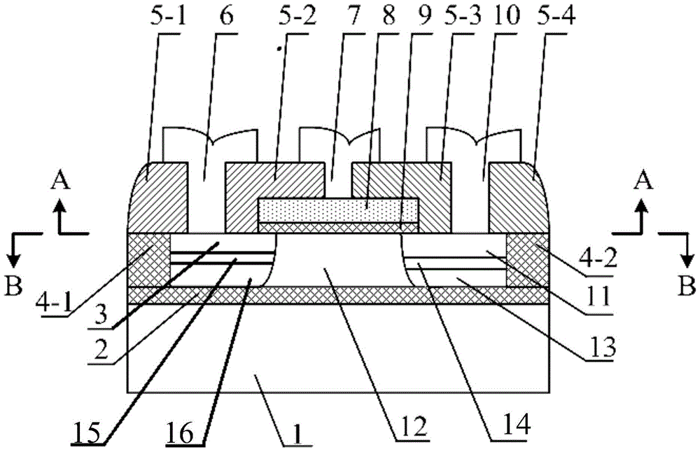
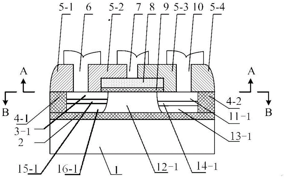
[0016] Such as figure 1 As shown, a drain-source region dielectric / PN junction isolation front gate P-MOSFET radio frequency switch ultra-low loss device based on SOI process, including P-type semiconductor substrate 1, buried oxide 2, N-type channel region 12, front gate P-type source region 3 of MOSFET, P-type drain region 11 of front gate MOSFET, P-type drain region 13 of back gate MOSFET, P-type drain isolation region 14, P-type source region 3 of front gate MOSFET, back gate MOSFET P-type drain region 16, P-type source region isolation region 15, deep trench isolation region (4-1, 4-2); buried oxide layer 2 is covered on P-type semiconductor substrate 1, and N-type channel region 12 is set On the buried oxide layer 2, deep trench isolation regions (4-1, 4-2) are arranged on the buried oxide layer 2 and surround the N-type channel region 1...


PUM


Abstract

The invention discloses a drain-source area medium / PN junction isolated front-gate P / N-MOSFET (Metal-Oxide-Semiconductor Field Effect Transistor) radio frequency switch ultralow-loss device based on an SOI (Silicon On Insulator) technology, wherein SOIP(N)-MOSFET device source and drain regions are modified, PN junctions or dielectric capacitors are produced in the source and drain regions, the junctions in source regions are large in depth, N(P) type doping or mediums are implanted in the source regions to form PN junctions or dielectric capacitors so as to form isolation to the voltage of direct current applied by a drain; through the biasing arrangement of the MOS and back-gate, the back-gate MOSFET channel is in a conducting state, altering current signals at the front-gate P(N)-MOSFET drain region are coupled to back-gate MOSFET; since the back-gate works in the conducting state, adjustment to impedance in ON state of the front-gate MOSFET is formed due to the structure, so that the radio frequency loss of the front-gate MOSFET serving as the switch applying to the ON state is reduced; when the back-gate MOSFET device generates negative impedance due to that the device generates self-heating effect, and the back-gate MOSFET works in the amplification state, front-gate coupling signals is directly amplified, energy loss in the ON state of the front-gate is compensated, and thus the ultrlow / zero-loss radio frequency switch is formed.

Description

technical field [0001] The invention belongs to the field of semiconductor technology, and relates to a radio frequency switch based on SOI (semiconductor-on-insulator technology drain-source region dielectric / diode isolation front gate P(N)-MOSFET (P(N) type metal-oxide-semiconductor transistor) ultra-low loss device. Background technique [0002] Due to the use of dielectric isolation, SOI P(N)-MOS devices eliminate the latch-up effect, and its unique insulating buried layer structure greatly reduces the parasitic effects of the device, greatly improving the performance of the circuit, with parasitic capacitance The advantages of small size, high integration density, fast speed, simple process, and small short channel effect are widely used in low voltage, low power consumption, high speed, radiation resistance, high temperature resistance and other fields. The structure of a conventional SOI P(N)-MOSFET device is a sandwich structure of an insulating substrate, a buried ...

Claims


Application Information

Patent Timeline
Patent Type & Authority Patents(China)
IPC IPC(8): H01L29/06
CPCH01L27/088H01L29/0646
Inventor 刘军
Owner HANGZHOU DIANZI UNIV
Why Eureka
Try Eureka