Method for manufacturing high-tension film and strain silicon metal oxide semiconductor transistor
A high-tension, strained silicon technology, applied in semiconductor/solid-state device manufacturing, electrical components, circuits, etc., can solve problems such as low tension, reduce the efficiency of ultraviolet technology, affect the drive current of thin-film stress metal oxide semiconductor transistors, etc., and achieve improvement The effect of stress
- Summary
- Abstract
- Description
- Claims
- Application Information
AI Technical Summary
Problems solved by technology
Method used
Image

Examples
Embodiment Construction
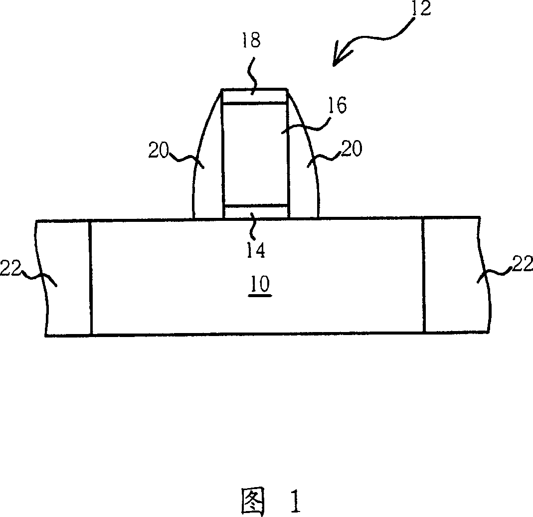
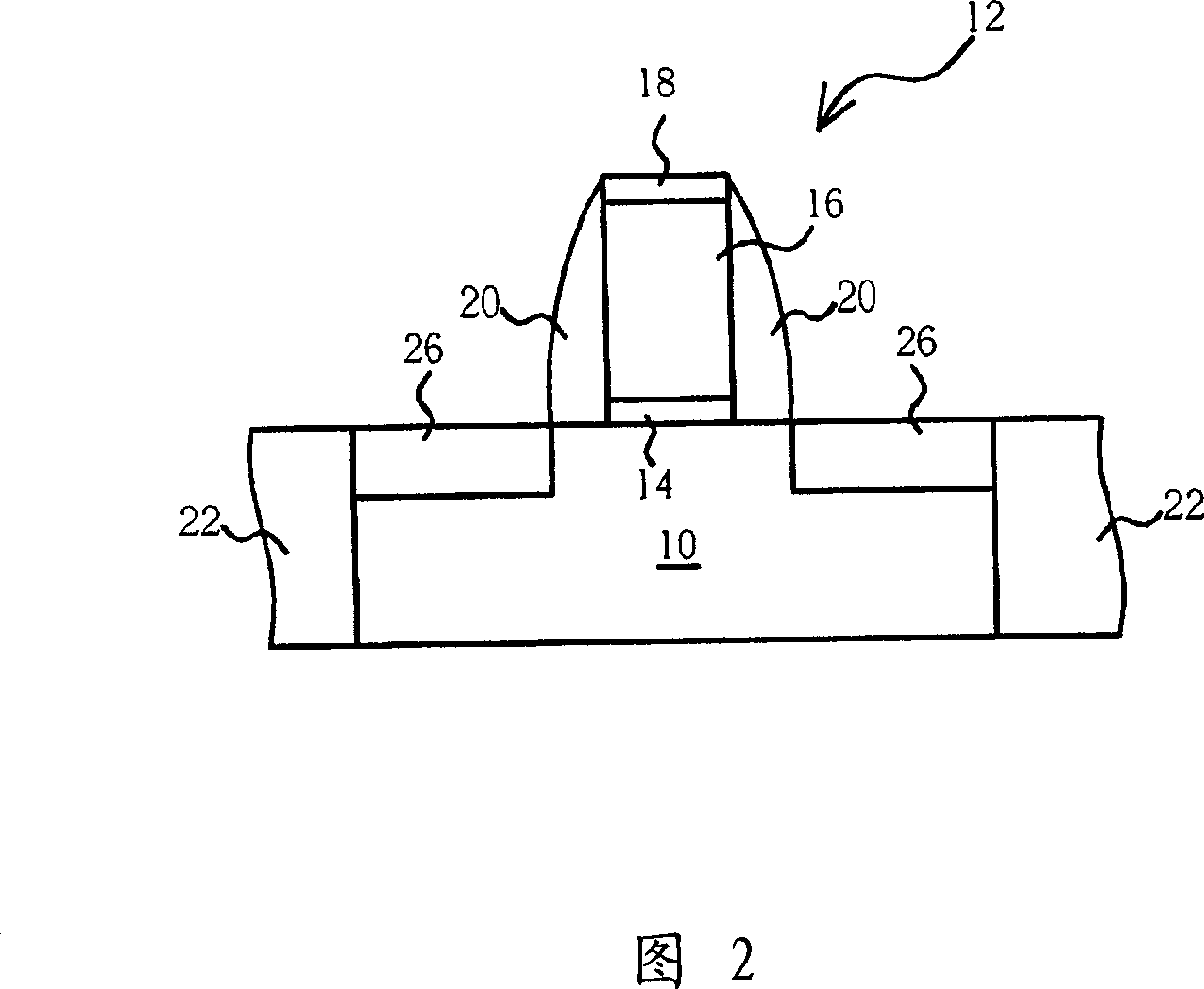
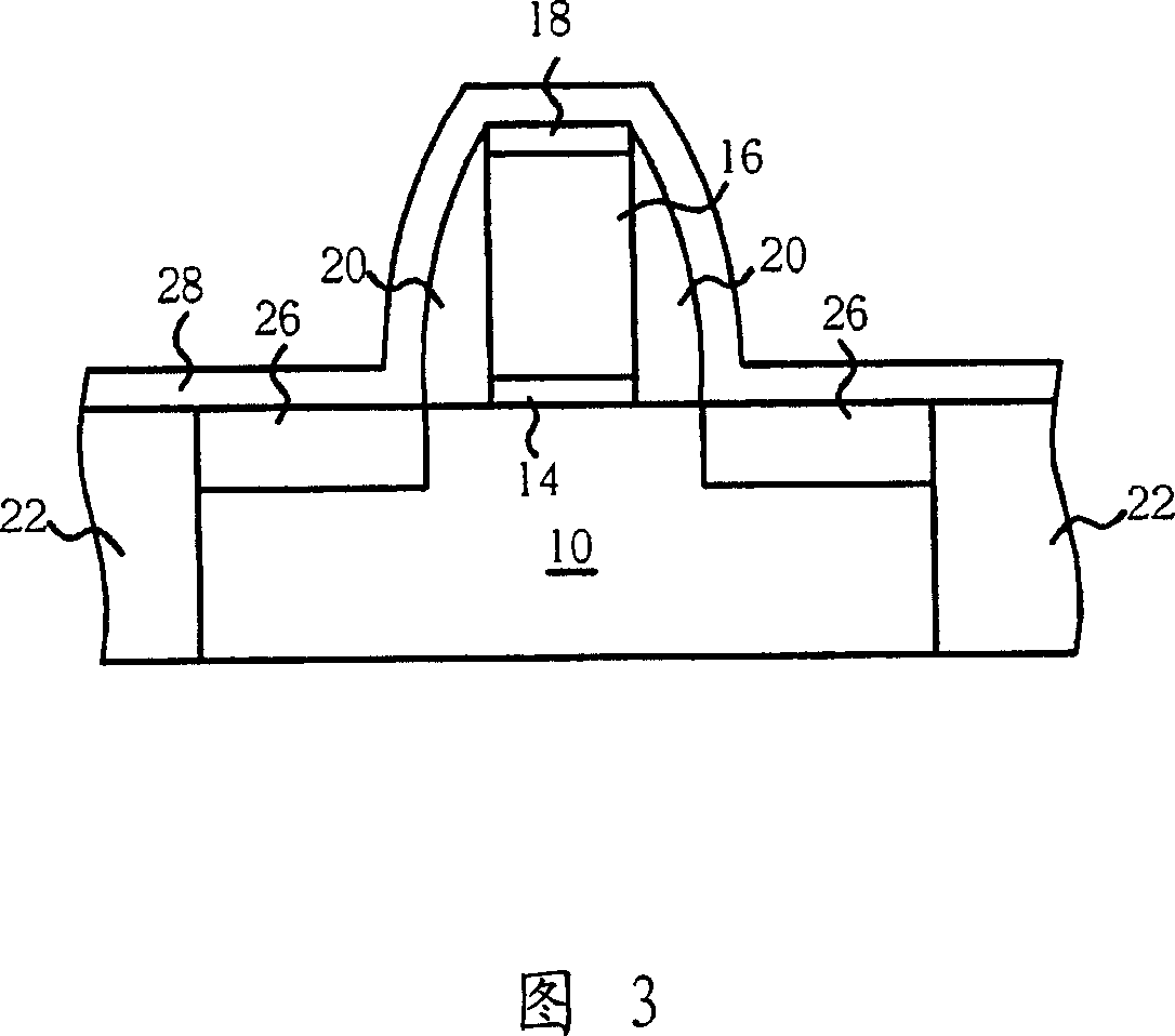
[0025] Please refer to FIG. 4 to FIG. 7 . FIG. 4 to FIG. 7 are schematic diagrams of a method for fabricating a high tension thin film on the surface of an NMOS transistor according to the present invention. As shown in FIG. 4 , firstly, a semiconductor substrate 60 is provided, such as a silicon wafer (wafer) or a silicon-on-insulator (SOI) substrate, and the semiconductor substrate 60 includes a gate structure 63 . Wherein, the gate structure 63 includes a gate dielectric layer 64, a gate 66 located on the gate dielectric layer 64, a cover layer 68 located on the top surface of the gate 66, and an oxide-nitride-oxide Offset spacer (ONO offset spacer) 70 . Generally speaking, the gate dielectric layer 64 can be made of a silicon oxide or silicon nitride compound formed by thermal oxidation or deposition, and the capping layer 68 can be made of a silicon nitride layer for protecting the gate 66. Or polycrystalline metal silicide (polycide) composition. In addition, the semic...
PUM
| Property | Measurement | Unit |
|---|---|---|
| Thickness | aaaaa | aaaaa |
| Wavelength | aaaaa | aaaaa |
Abstract
Description
Claims
Application Information
 - Generate Ideas
- Intellectual Property
- Life Sciences
- Materials
- Tech Scout
- Unparalleled Data Quality
- Higher Quality Content
- 60% Fewer Hallucinations
Browse by: Latest US Patents, China's latest patents, Technical Efficacy Thesaurus, Application Domain, Technology Topic, Popular Technical Reports.
© 2025 PatSnap. All rights reserved.Legal|Privacy policy|Modern Slavery Act Transparency Statement|Sitemap|About US| Contact US: help@patsnap.com