Semiconductor chip buried base plate 3D construction and its manufacturing method

A semiconductor and chip technology, applied in the field of three-dimensional packaging structure and its manufacturing method, can solve the problems of unstable quality of the overall packaging structure, difficulty in filling insulating materials, easy generation of air bubbles, etc., and achieve good quality and product reliability, The effect of improving the good rate and saving the cost

Active Publication Date: 2007-05-30
PHOENIX PRECISION TECH CORP
View PDF1 Cites 10 Cited by
  • Summary
  • Abstract
  • Description
  • Claims
  • Application Information

AI Technical Summary

Problems solved by technology

However, the gap is small, and it is difficult to fill it with insulating materials such as resin. During the filling process, air bubbles are easily generated in the gap, which will cause popcorn phenomenon in the subsequent heating process, resulting in unstable quality of the overall structure.

Method used


Image

  • Semiconductor chip buried base plate 3D construction and its manufacturing method
  • Semiconductor chip buried base plate 3D construction and its manufacturing method
  • Semiconductor chip buried base plate 3D construction and its manufacturing method

Examples


Embodiment 1

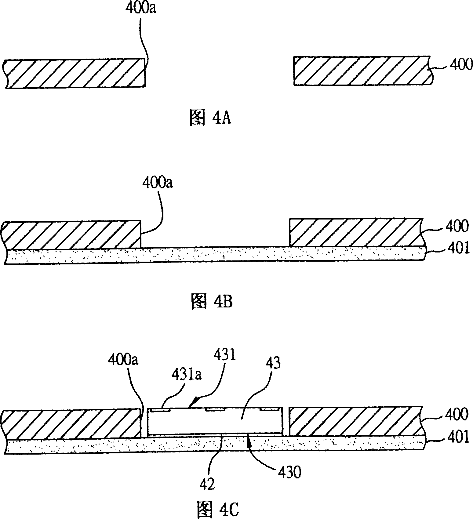
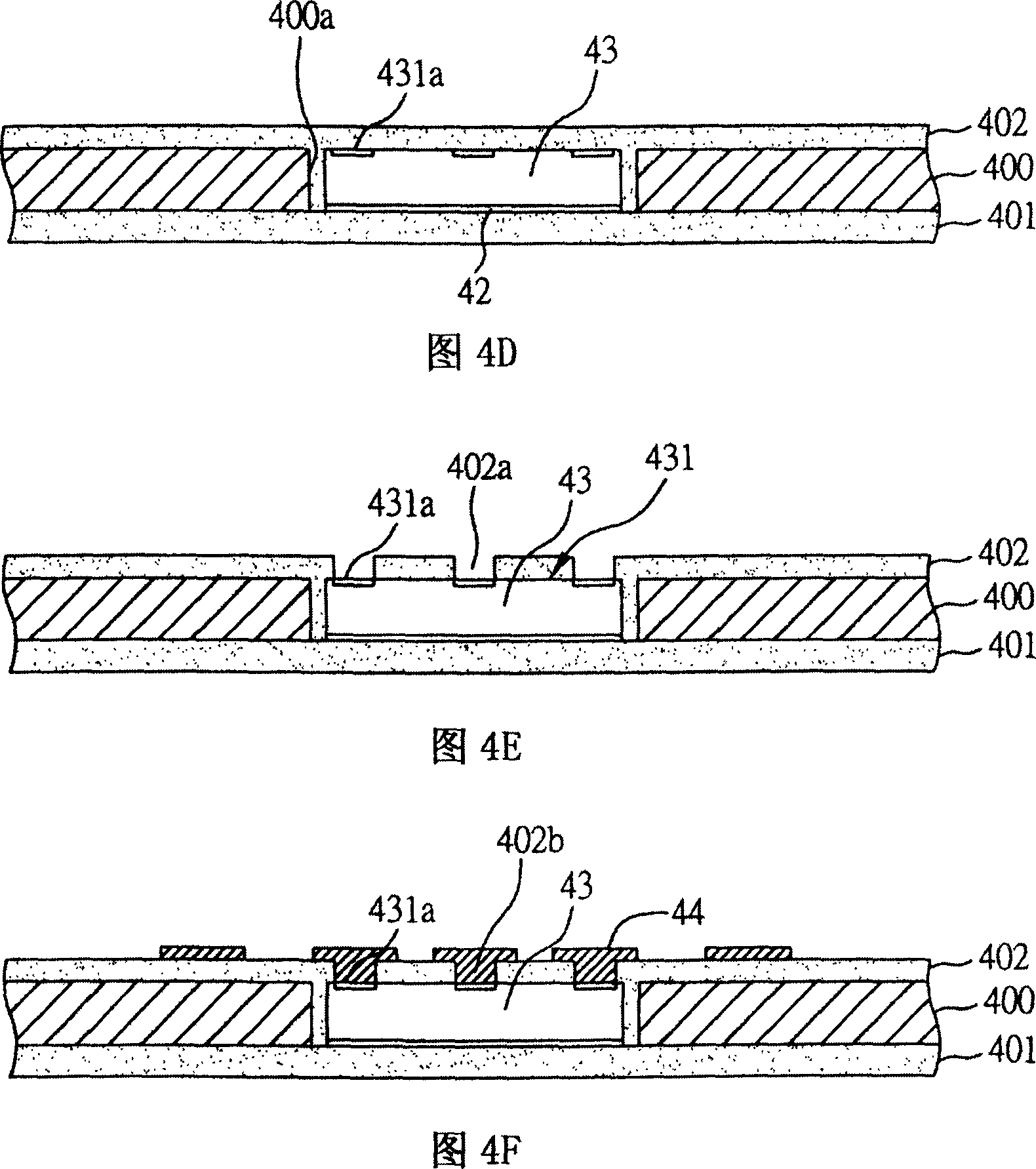
[0026] Please refer to FIGS. 4A to 4F , which are schematic cross-sectional views of Embodiment 1 of the manufacturing method of the semiconductor package structure of the present invention.

[0027] Referring to FIG. 4A , firstly, a carrier 400 having a through hole 400 a is provided. The carrier 400 can be an insulating core board, a metal plate or a circuit board with circuits, and the thickness of the carrier 400 can be determined as required.

[0028] Please refer to FIG. 4B , and then the carrier 400 is bonded on the first insulating layer 401 . The first insulating layer 401 can be prepreg (prepeg) or film (film) material, such as epoxy resin (epoxy resin), polyimide (polyimide), LCP, bismaleimide triazine ( BT, Bismaleimide triazine), ABF (Ajinomoto Build-up Film), polyphenylene ether (PPE), polytetrafluoroethylene (PTFE), benzocyclobutene (BCB, benzocylobutene), etc. The first insulating layer 401 is not fully cured insulating layer.

[0029]Referring to FIG. 4C , ...

Embodiment 2

[0035] Please refer to FIGS. 5A to 5H , which are schematic cross-sectional views of Embodiment 2 of the manufacturing method of the semiconductor package structure of the present invention. Embodiment 2 of the semiconductor assembly structure and its manufacturing method of the present invention is similar to Embodiment 1, the main difference is that a heat dissipation blind hole connected to the non-circuit surface of the semiconductor chip is formed in the first insulating layer, and the heat dissipation blind hole is filled with heat dissipation The material and the heat conduction circuit layer connected to the circuit structure are connected to the outside, and it can further provide direct external connection with other heat dissipation devices, so as to further improve the heat dissipation effect of the semiconductor package structure.

[0036] Referring to FIG. 5A , firstly, a carrier 500 having a through hole 500 a is provided. The carrier 500 can be an insulating co...


PUM


Abstract

This invention relates to semiconductor chip imbed baseboard three dimensional seal structure and its process method, which comprises the following steps: connecting load parts with at least one hole to first insulation layer and at least one conductor chip onto first insulation contained in the load holes; then forming second insulation layer onto load part and chips for adhesion and filling insulation resin into gap between load board and chip to form electricity connection to chip circuit layer; forming chip dissipation blind hole on first insulation layer to aid semiconductor chip to dissipate heat outside.

Description

technical field [0001] The present invention relates to a three-dimensional assembly structure of semiconductor chips embedded in a substrate and a manufacturing method thereof, in particular to a semiconductor assembly structure integrating a chip and a carrier and a manufacturing method thereof. Background technique [0002] With the vigorous development of the electronic industry, electronic products have gradually entered the direction of multi-functional and high-performance research and development. In order to meet the packaging requirements of high integration and miniaturization of semiconductor packages, circuit boards that provide multiple active and passive components and line connections have gradually evolved from single-layer boards to multi-layer boards ( Multi-layer board), in a limited space, expand the available circuit area on the circuit board by means of interlayer connection technology to meet the needs of high-density integrated circuits (Integrated c...

Claims


Application Information

Patent Timeline
Patent Type & Authority Applications(China)
IPC IPC(8): H01L21/50H01L23/31H01L23/488H01L23/36
CPCH01L2924/0002H01L2224/2518H01L24/19H01L2224/16225H01L2224/04105H01L2224/12105H01L2224/19H01L2224/73267H01L2924/14H01L2924/00H01L2924/00012
Inventor 许诗滨
Owner PHOENIX PRECISION TECH CORP
Why Eureka
Try Eureka