
Die bonding adhesive tape

A chip bonding and adhesive tape technology, applied in the direction of adhesives, film/sheet adhesives, heat-activated films/sheets, etc., can solve the problem of not significantly reducing the adhesion, increasing the difficulty of picking up chips, and destroying chips And other issues

Active Publication Date: 2007-06-13
ACE IND CO LTD
View PDF0 Cites 7 Cited by
  • Summary
  • Abstract
  • Description
  • Claims
  • Application Information

AI Technical Summary

Problems solved by technology

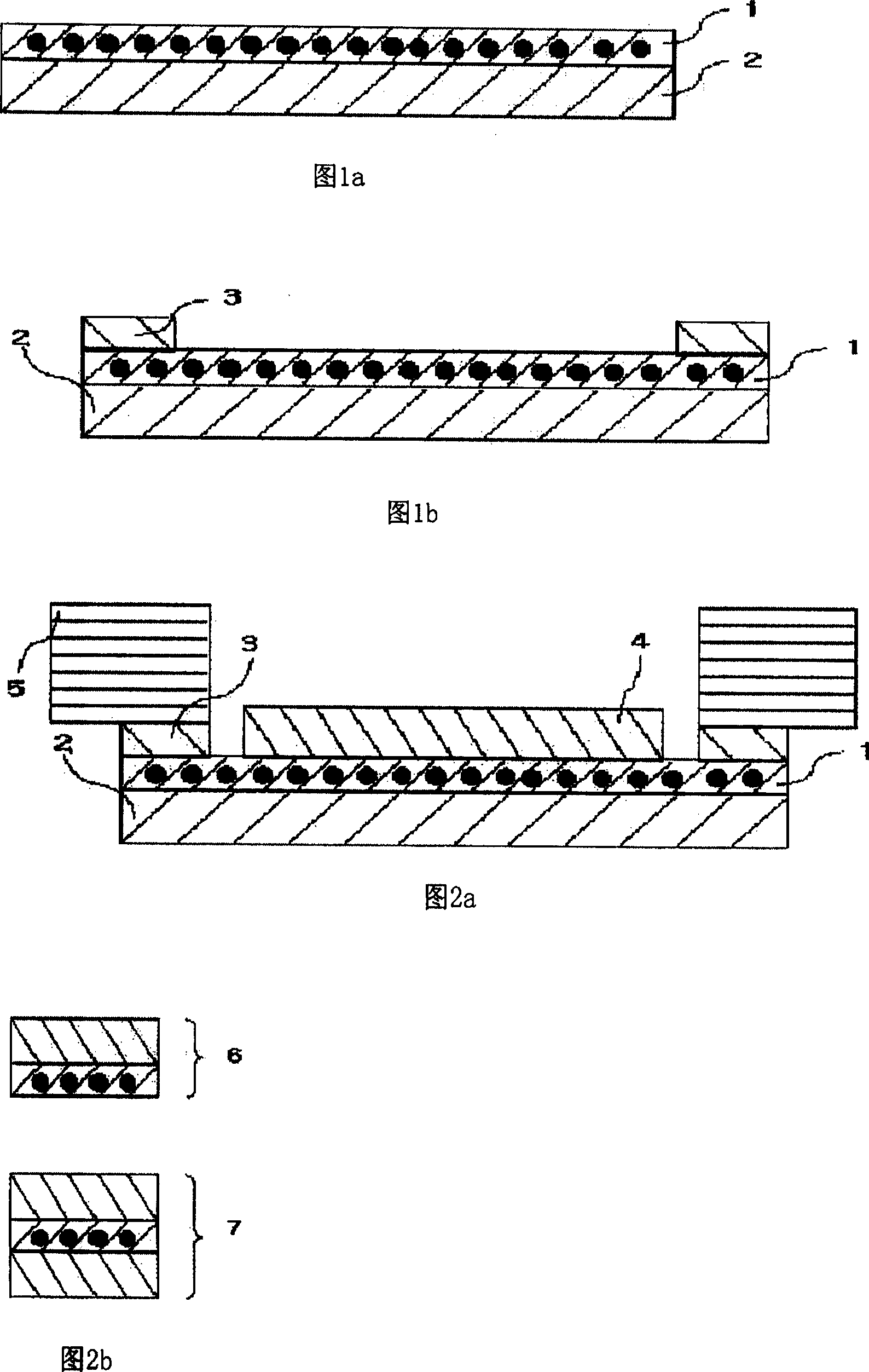
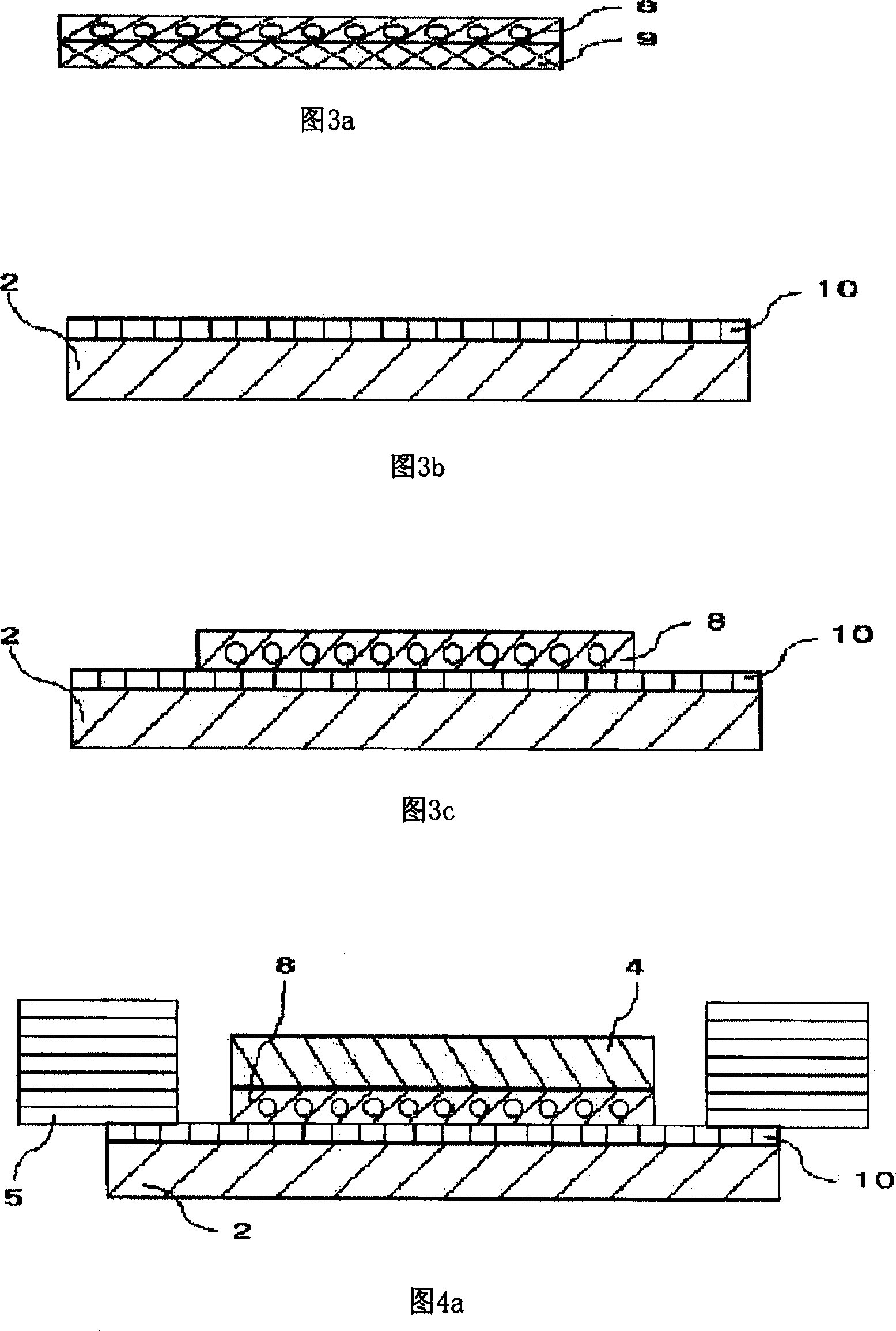
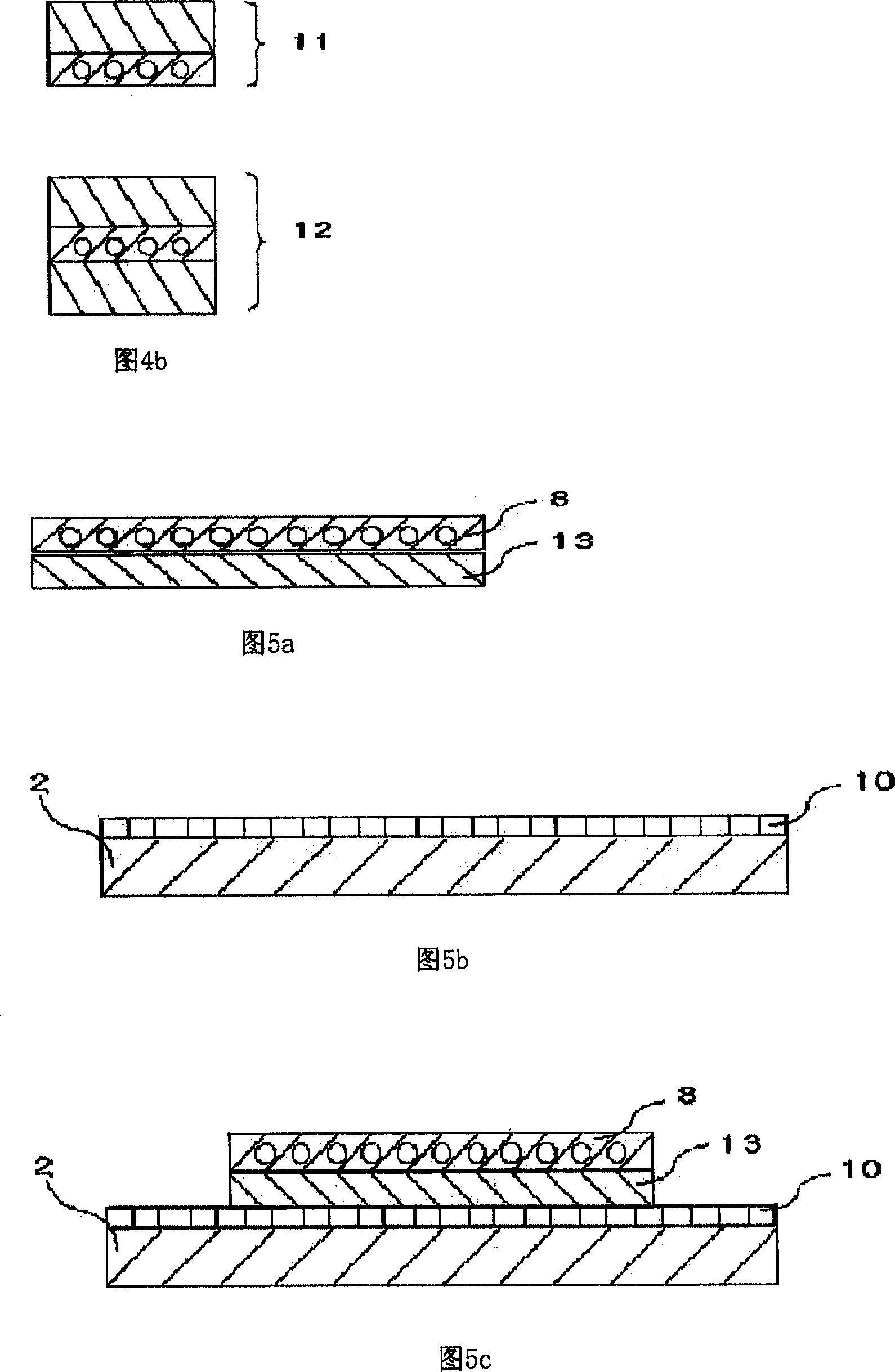
However, since most of the UV-curable low-molecular-weight compounds of the adhesive layer (10) have been transferred and diffused into the adhesive layer (8) before the ultraviolet light irradiation, the adhesiveness cannot be significantly reduced when the ultraviolet light is irradiated. Attachment
In addition, when the chip size is not smaller than 10 mm × 10 mm and the thickness is 75 μm or less, the adhesive force between the adhesive film adhered to the chip and the adhesive layer on the substrate is not significantly reduced, thus increasing the difficulty of chip pickup
In addition, when the chip pick-up process is barely performed, the chip will be damaged due to the pick-up pressure, which is not desirable
In addition, described phenomenon also occurred in prior art one
Therefore, the adhesive tapes disclosed in prior art 1 and prior art 2 have many limitations when picking up thin and large chips

Method used


Image

  • Die bonding adhesive tape
  • Die bonding adhesive tape
  • Die bonding adhesive tape

Examples


manufacture example 1

[0049] [Manufacturing example 1] Manufacture of die-bonding adhesive film 1

[0050] An acrylic curing agent and a curing accelerator are added to a die-bonding adhesive film composition composed of an epoxy resin, a phenolic resin, and an acrylic adhesive solution to cure the epoxy resin. In this way, the epoxy resin and the phenolic resin were mixed at a ratio of 5:3 and stirred for 30 minutes, and then the resulting stirred solution and the acrylic adhesive were mixed at a ratio of 15:45 and stirred for 3 hours. Then add an acrylic curing agent and an epoxy curing accelerator therein and continue stirring for 30 minutes to form a die-bonding adhesive film 1 . As shown in Composition Table 1 below, each component was used after being diluted in an organic solvent at a predetermined ratio.

manufacture example 2

[0051] [Manufacturing example 2] Manufacture of die-bonding adhesive film 2

[0052] The method of manufacturing the die-bonding adhesive film was the same as that of Production Example 1, and then added a UV-curable low-molecular-weight compound in order to increase the adhesion and stirred for 30 minutes to prepare the die-bonding adhesive film 2 .

manufacture example 3

[0053] [Manufacturing example 3] Manufacture of die-bonding adhesive film 3

[0054] The method for producing the die-bonding adhesive film was the same as in Production Example 2, and then a photoinitiator was added for ultraviolet light curing, followed by stirring for 30 minutes to produce a die-bonding adhesive film 3 .


PUM

PropertyMeasurementUnit
thicknessaaaaaaaaaa
surface tensionaaaaaaaaaa
thicknessaaaaaaaaaa

Abstract

Disclosed is a die bonding adhesive tape, which eliminates the requirement for additional adhesive tape for attaching a ring frame, decreases the curing time period upon die bonding, essentially prevents the transfer and diffusion of low-molecular-weight compounds between an adhesive film and an adhesive layer on a base substrate to thus exhibit excellent pick-up performance when picking up a die, and easily separates an adhesive film having a die from an adhesive layer on a base substrate when picking up slim and large dies. The die bonding adhesive tape of the invention includes a base substrate and an adhesive layer formed on the base substrate, has a structure in which a core film having a die bonding adhesive film attached thereto is bonded onto the adhesive layer, and enables direct die bonding via dicing and then die pick-up in a state of being mounted on a wafer.

Description

technical field [0001] The present invention relates generally to a die-bonding adhesive tape, and more particularly, to a die-bonding adhesive tape for improving work efficiency and shortening work time in a semiconductor manufacturing process. Background technique [0002] In the semiconductor manufacturing process, a wafer having a large diameter is disassembled into small chips after a dicing process, and the disassembled chiplets are subjected to a series of processes including cleaning, drying, expanding, picking, and bonding with a lead frame. In this way, an adhesive tape is used in order to prevent chip splashing in the dicing process. While the adhesive tape needs to be strong enough to hold the die from the slicing process to the drying process, its adhesion should be significantly reduced during the pick-up process so that the die can be safely transferred to the die-bonding process. process. [0003] Further, in the die bonding process, the chip transferred to...

Claims


Application Information

Patent Timeline
Patent Type & Authority Applications(China)
IPC IPC(8): C09J7/02C09J7/35
CPCH01L24/29H01L24/27C09J2409/00H01L2924/01027H01L24/83H01L2224/2919C09J2203/326H01L2924/01013H01L2924/01005H01L2924/01082H01L2924/01033H01L2224/8385H01L2224/274H01L2224/83191H01L2221/68327H01L2924/01015C09J7/0203H01L2924/0665H01L2924/01006C09J2433/00H01L21/6836H01L2924/07802H01L2924/14C09J2463/00C09J7/021C09J7/35C09J7/381H01L2924/00H01L2924/3512H01L23/14
Inventor 安镛国沈昌勋潢教圣
Owner ACE IND CO LTD
Learn More