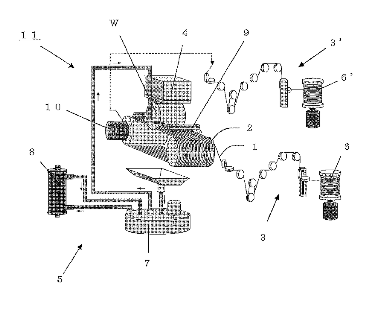
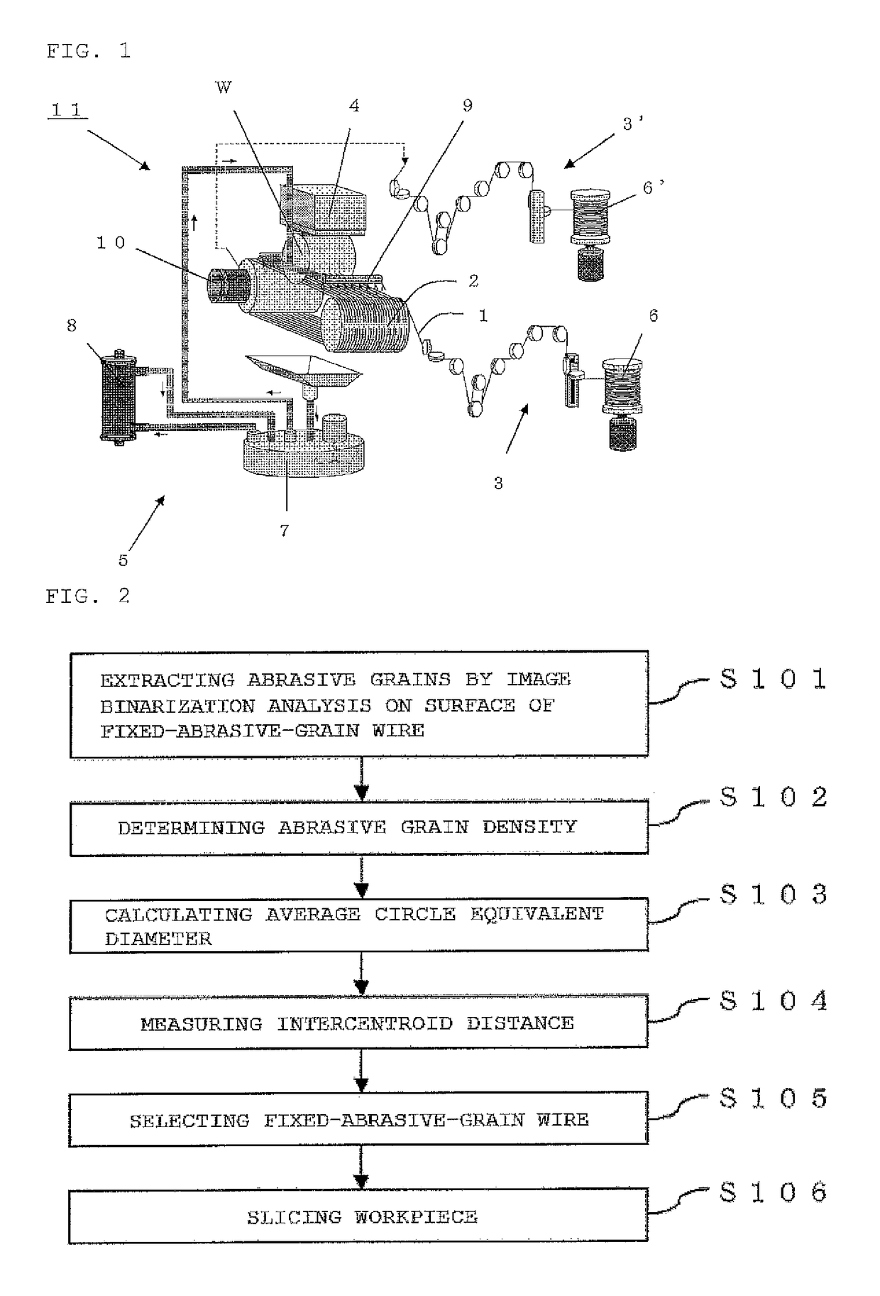
Fixed-abrasive-grain wire, wire saw, and method for slicing workpiece
a technology of fixed abrasive grains and wire saws, which is applied in the direction of metal sawing apparatus, grinding machines, manufacturing tools, etc., can solve the problems of reducing the productivity per wafer, and the integration of semiconductor devices such as dram, nand flash memory, and mpu approaches technical limits, so as to improve the shape accuracy and shorten the slicing time , the effect of high productivity
- Summary
- Abstract
- Description
- Claims
- Application Information
AI Technical Summary
Benefits of technology
Problems solved by technology
Method used
Image

Examples
example 1
[0093]A fixed-abrasive-grain wire selected in accordance with the inventive method for slicing a workpiece shown in FIG. 2 was attached to a wire saw shown in FIG. 1. A workpiece was sliced with the wire saw in accordance with the inventive method for slicing a workpiece. Then, TTV and warp of all wafers sliced from the workplace were measured and their average values were calculated.
[0094]The fixed-abrasive-grain wire used in this example had a core wire with a diameter of 0.1 mm and diamond abrasive grains fixed to the core wire with a particle size distribution in which a minimum diameter was 6 μm and a maximum diameter was 12 μm.
[0095]The fixed-abrasive-grain wire had an abrasive grain density of 1200 grains / mm2, and 0.9% of all distances between centroids of the abrasive grains were equal to or shorter than an average circle equivalent diameter of the whole abrasive grains. An image of the surface of the fixed-abrasive-grain wire was taken with a scanning electron microscope. T...
example 2
[0100]A silicon single crystal ingot was sliced under the same condition as in example 1 except that the used fixed-abrasive-grain wire had an abrasive grain density of 1500 grains / mm2, and 2.0% of all distances between centroids of the abrasive grains were equal to or shorter than an average circle equivalent diameter of the whole abrasive grains. Then, average TTV and warp of all sliced-out wafers were calculated.
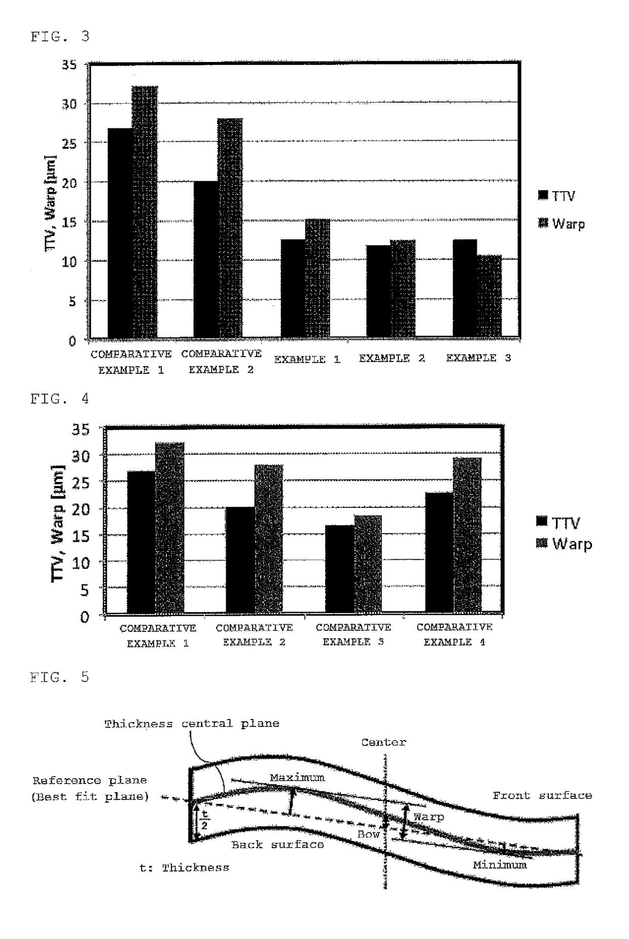
[0101]Consequently, as shown in Table 2 and FIG. 3, the wafers had an average TTV of 11.8 (μm) and an average warp of 12.5 (μm); thus the obtained wafers had much better shape accuracy than those in comparative examples described later.
example 3
[0102]A silicon single crystal ingot was sliced under the same condition as in example 1 except that the used fixed-abrasive-grain wire had an abrasive grain density of 1500 grains / mm2, and 1.5% of all distances between centroids of the abrasive grains were equal to or shorter than an average circle equivalent diameter of the whole abrasive grains. Then, average TTV and warp of all sliced-out wafers were calculated.
[0103]Consequently, as shown in Table 2 and FIG. 3, the wafers had an average TTV of 12.43 (μm) and an average warp of 10.45 (μm); thus the obtained wafers had much better shape accuracy than those in comparative examples described later. These TTV and warp values were equal to shape quality obtained by slicing in the loose-abrasive-grain manner (see FIG. 6). This confirms that the present invention, which uses the fixed-abrasive-grain wire, can significantly shorten the slicing time and yield wafers with shape accuracy equal to those obtained with loose abrasive grains. ...
PUM
| Property | Measurement | Unit |
|---|---|---|
| grain diameter | aaaaa | aaaaa |
| grain diameter | aaaaa | aaaaa |
| grain diameter | aaaaa | aaaaa |
Abstract
Description
Claims
Application Information
 - R&D
- Intellectual Property
- Life Sciences
- Materials
- Tech Scout
- Unparalleled Data Quality
- Higher Quality Content
- 60% Fewer Hallucinations
Browse by: Latest US Patents, China's latest patents, Technical Efficacy Thesaurus, Application Domain, Technology Topic, Popular Technical Reports.
© 2025 PatSnap. All rights reserved.Legal|Privacy policy|Modern Slavery Act Transparency Statement|Sitemap|About US| Contact US: help@patsnap.com