RF switch with split tunable matching network

a technology of rf switch and matching network, which is applied in the direction of amplifier types, amplifiers, amplifiers with semiconductor devices/discharge tubes, etc., can solve the problems of reducing output power and efficiency, affecting the performance of the edge of the frequency band, and unable to meet all design requirements. , to achieve the effect of good power output and efficiency, good bandwidth, and good tunability and design flexibility

Active Publication Date: 2018-07-31
PSEMI CORP
View PDF8 Cites 8 Cited by
  • Summary
  • Abstract
  • Description
  • Claims
  • Application Information

AI Technical Summary

Benefits of technology

[0011]The present invention encompasses an improved architecture for a radio frequency (RF) power amplifier, impedance matching network, and selector switch that allows for good tunability and design flexibility over a desired range of frequency bands, good bandwidth, good power output and efficiency, low loss, easy adjustability, low cost, and faster time-to-market. One aspect of embodiments of the invention is splitting the functionality of a final stage impedance matching network (IMN) into two parts, comprising a base set of off-chip IMN components and an on-chip IMN tuning component.
[0013]Embodiments of the invention need not be integrated with a power amplifier. For example, a first integrated circuit may include an on-chip IMN tuner and a selector switch, and be configured to be coupled to an off-chip set of IMN components and to a second integrated circuit having an RF power amplifier. Separating the off-chip set of IMN components and the on-chip IMN tuner of the first IC from the RF power amplifier of the second IC allows selection of a particularly well suited fabrication technology for each element of the system, while providing the benefits of integration and tunability.
[0014]Splitting the functionality of a final stage impedance matching network for an RF power amplifier into two parts, as well as placing the on-chip IMN tuner in close proximity to the selector switch, provide important advantages, including (among others): the off-chip set of IMN components can be fabricated inexpensively compared to on-chip counterparts, in large part because on-chip inductors of a size sufficient to provide good bandwidth and efficiency take up a large amount of IC die area, and can generally be more efficient than an on-chip implementation; the close proximity of the on-chip IMN tuner to the selector switch allows impedance match tuning that takes into account all of the parasitic elements between the PA final stage and the selector switch, such as the parasitic inductance, capacitance, and / or resistance of the bonding wires to the off-chip set of IMN components; the on-chip IMN tuner of the final stage IMN can be adjusted to accommodate the imperfect input impedance of coupled band filters or even antenna impedance; with an on-chip IMN tuner, such as a DTC, the operating frequencies of the final stage IMN can be made wider; the selector switch and the on-chip IMN tuner (particularly if implemented as a DTC) may be integrated on the same die using the same technology; because the bulk of the final stage IMN components are off-chip, different off-chip IMN components can be utilized with a common IC having a selector switch and an on-chip IMN tuner, thus allowing a single IC to be used for multiple different applications, thereby reducing time-to-market; splitting the functionality as described below enables the use of a split final stage IMN with any PA device fabrication technology; and embodiments of the invention can reduce total die area on an IC by sharing control logic and other analog / digital circuitry with the on-chip IMN tuner and the selector switch.

Problems solved by technology

In light of the number of parameters affecting the design of an IMN, it is often difficult to synthesize a fixed (non-tunable) IMN that simultaneously fulfills all design requirements while providing enough bandwidth to cover a desired range of operating frequencies.
Often performance at the edges of frequency bands suffers when attempting to make a wideband IMN.
This architecture provides quite good tunability and few off-chip parasitic elements (e.g., bonding wire parasitic inductance, capacitance, and / or resistance), but may have lower output power and efficiency due to lossy integrated inductors within the final stage IMN 112.
Further, the inclusion of on-chip inductors increases the overall circuit size, and thus the cost of integrated circuit fabrication, and may limit the range of tunability.
However, off-chip implementation of the final stage IMN 212 introduces parasitic elements that are generally difficult to counteract in order to achieve good performance and meet design criteria.

Method used


Image

  • RF switch with split tunable matching network
  • RF switch with split tunable matching network
  • RF switch with split tunable matching network

Examples


Embodiment Construction

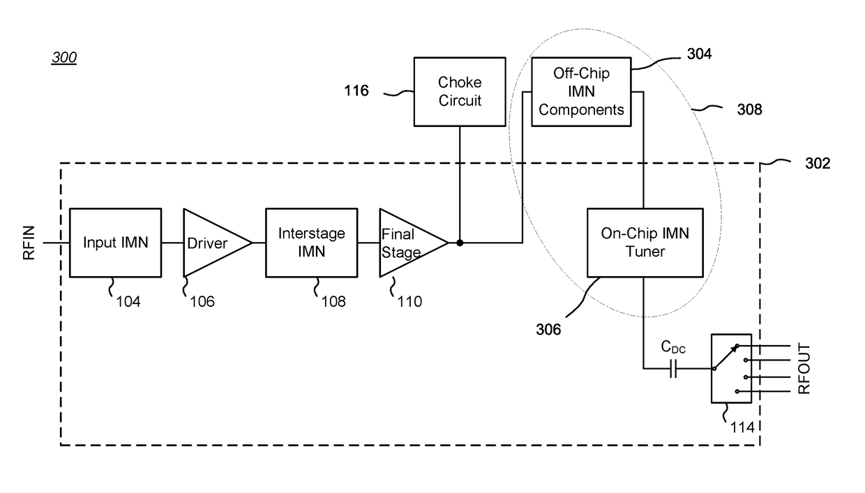
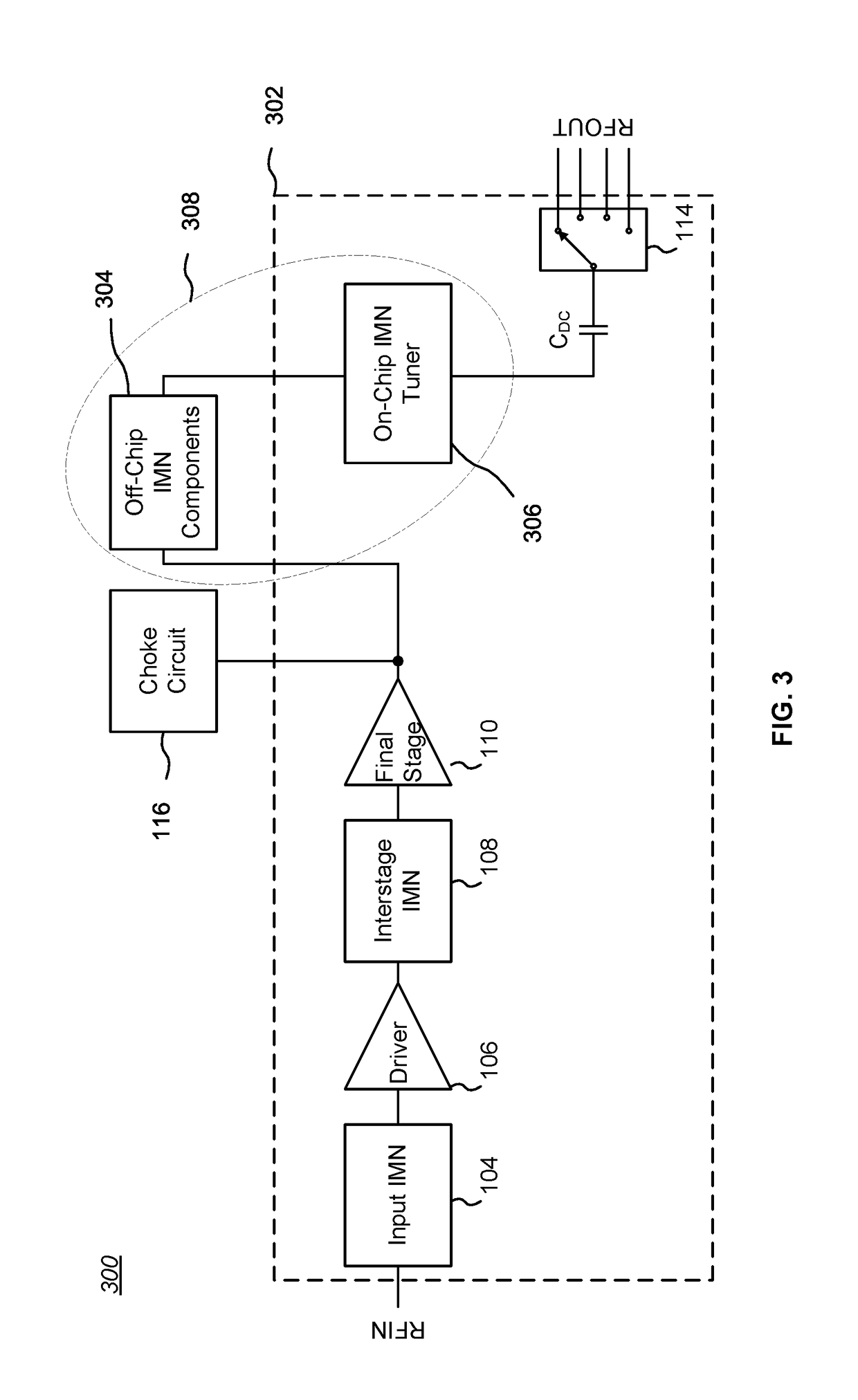
[0025]The present invention encompasses an improved architecture for a radio frequency (RF) power amplifier, impedance matching network, and selector switch that allows for good tunability and design flexibility over a desired range of frequency bands, good bandwidth, good power output and efficiency, low loss, easy adjustability, low cost, and faster time-to-market. One aspect of embodiments of the invention is splitting the functionality of a final stage impedance matching network (IMN) into two parts, comprising a base set of off-chip IMN components and an on-chip IMN tuning component.

[0026]Single-IC Split IMN Architecture

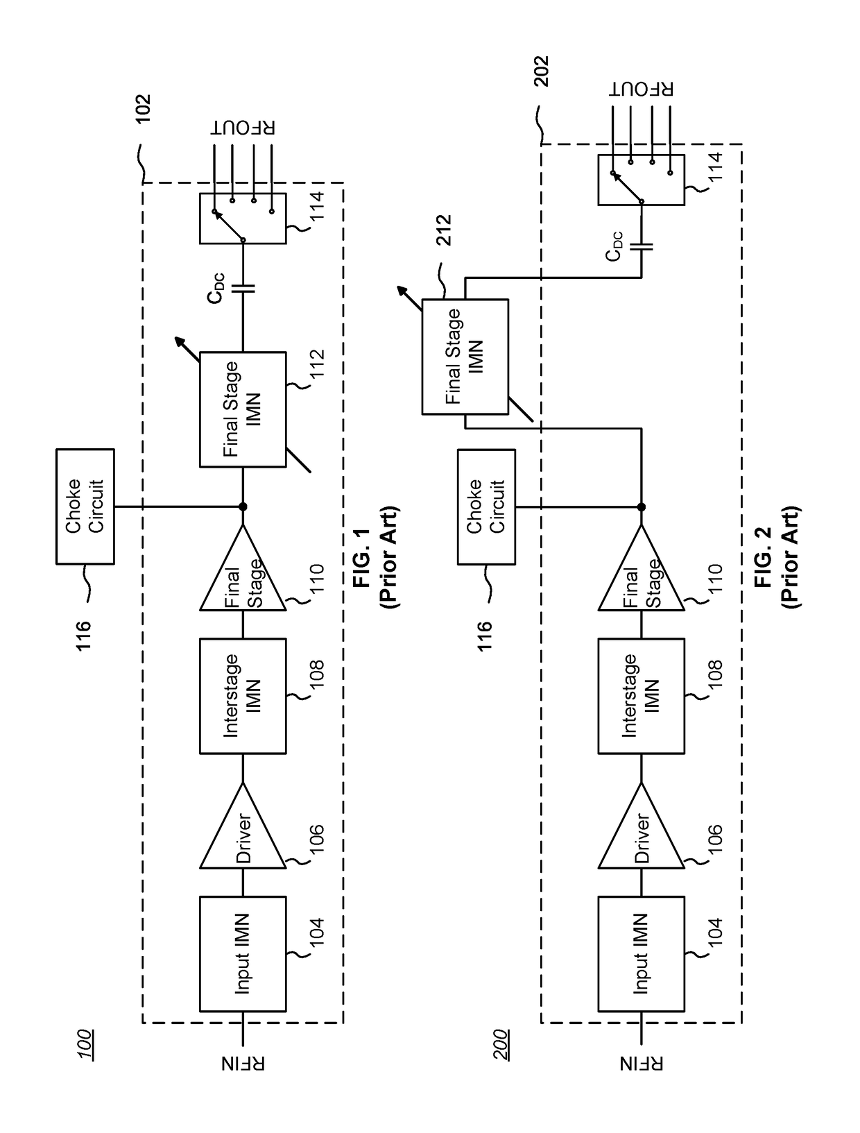
[0027]FIG. 3 is a block diagram of a RF power amplifier 300 having a general split IMN architecture. Similar to FIG. 1 and FIG. 2, an integrated circuit (IC) 302 includes several subcircuits that accept an RF input signal RFIN and output an amplified and impedance matched output signal RFOUT to a selected destination (e.g., one or more antennas, duplexers, band ...


PUM


Abstract

An improved architecture for a radio frequency (RF) power amplifier, impedance matching network, and selector switch. One aspect of embodiments of the invention is splitting the functionality of a final stage impedance matching network (IMN) into two parts, comprising a base set of off-chip IMN components and an on-chip IMN tuning component. The on-chip IMN tuning component may be a digitally tunable capacitor (DTC). In one embodiment, an integrated circuit having a power amplifier, an on-chip IMN tuner, and a selector switch is configured to be coupled to an off-chip set of IMN components. In another embodiment, an integrated circuit having an on-chip IMN tuner and a selector switch is configured to be coupled through an off-chip set of IMN components to a separate integrated circuit having an RF power amplifier.

Description

BACKGROUND(1) Technical Field[0001]This invention relates to electronic radio frequency power amplifier and selector switch circuitry.(2) Background[0002]Typical electronic power amplifiers use fixed output impedance matching networks (IMNs) to transform the low impedance of the power amplifier device (e.g., 3 ohms) to the characteristic impedance of an electronic system as a whole (e.g., 50 ohms, for modern radio frequency circuitry). IMNs can be built using a variety of architectures, including lumped elements (e.g., inductors and capacitors), distributed elements (e.g., transmission lines), and / or transformers.[0003]The circuit architecture, topology, and component values of IMNs are generally selected to provide desired performance parameters, such as impedance transformation (e.g., from 3 ohms to 50 ohms), frequency response (e.g., low pass), and harmonic termination (e.g., presenting a short circuit at the second harmonic frequency, 2f0, of the fundamental system frequency f0,...

Claims


Application Information

Patent Timeline
Patent Type & Authority Patents(United States)
IPC IPC(8): H03F1/56H03F3/21H03F3/19
CPCH03F1/56H03F3/19H03F3/21H03F2200/451H03F2200/387H03F3/195H03F3/213H03F2200/378
Inventor RANTA, TERO TAPIOCHENG, CHIH-CHIEHROBERTS, KEVIN
Owner PSEMI CORP
Why Eureka
Try Eureka