Virtual cathode deposition (VCD) for thin film manufacturing

a virtual cathode and film manufacturing technology, applied in the direction of discharge tube/lamp details, discharge tube main electrode, discharge tube hollow cathode, etc., can solve the problems of low reproducibility of pulses from shot to shot, failure of csd electron beam source for industrial applications, and failure of pulsed electron beam for thin film deposition

Active Publication Date: 2018-08-14
META MATERIALS INC
View PDF7 Cites 4 Cited by
  • Summary
  • Abstract
  • Description
  • Claims
  • Application Information

AI Technical Summary

Benefits of technology

[0005]A new type of thin film deposition apparatus and method are proposed. The deposition apparatus operation is based on application high voltage (1-60 kV) high current (0.1-10 kA) electrical pulse, generated by a pulsed power group, to a virtual cathode group. The virtual cathode group apparatus generates initial plasma from a gas supplied in a gas container. This initial plasma, being injected in front of target, forms a virtual plasma cathode. This virtual cathode plasma obtains a negative potential bias, provided by the pulsed power supply, that leads to generation of an electron beam. The formation of the electron beam occurs in the thin sheath which is formed between the boundary of the plasma serving as virtual cathode and the target serving as an anode. Due to the small distance between the plasma boundary and target the space-charge limit is high and this allows high-energy and high-current pulsed electron beam generation, sufficient for the solid target ablation.
[0006]The virtual plasma cathode appears temporarily in front of the target, ablates it with electron beam, and then disappears allowing the ablated material of target to propagate towards the substrate, where it condenses to form a thin film. The ablated material, in a form of a plasma plume, propagates outward the target surface through the section where the virtual cathode plasma was located. In this way, the factor restricting the uptime of electron beam sources—contamination of the cathode by the ablated material—is avoided because the cathode is a virtual one, formed from plasma and it cannot become contaminated in the way that a conventional solid material cathode can.

Problems solved by technology

In spite of successful deposition experiments in a number of worldwide laboratories, there is as yet no successful industrial application of the pulsed electron beam for deposition of thin films.
The main reason that the electron beam source based on CSD has failed for industrial applications is because of the short life-time (generally 8 shots) of the dielectric tubular element, low reproducibility of the pulses from-shot-to-shot, and scalability problems for wide area deposition.

Method used


Image

  • Virtual cathode deposition (VCD) for thin film manufacturing
  • Virtual cathode deposition (VCD) for thin film manufacturing
  • Virtual cathode deposition (VCD) for thin film manufacturing

Examples


Embodiment Construction

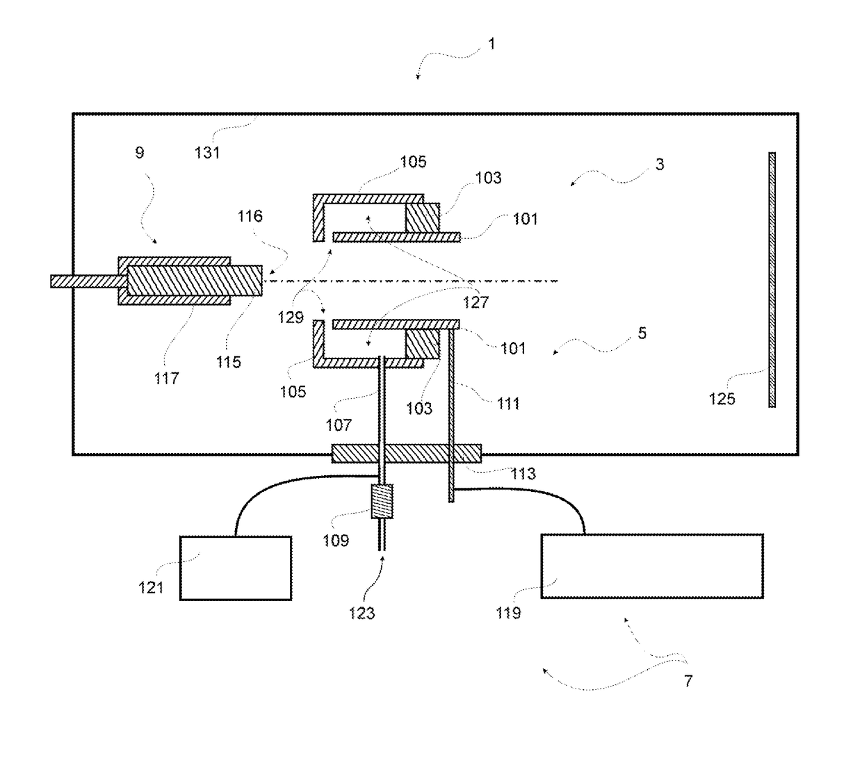
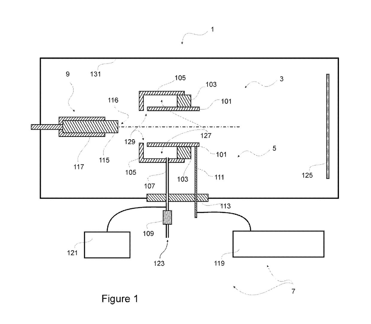
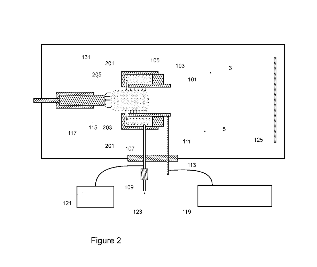
[0047]With specific reference now to the drawings in detail, it is stressed that the particulars shown are by way of example and for purposes of illustrative discussion of the preferred embodiments of the present invention only, and are presented in the cause of providing what is believed to be the most useful and readily understood description of the principles and conceptual aspects of the invention. In this regard, no attempt is made to show structural details of the invention in more detail than is necessary for a fundamental understanding of the invention, the description taken with the drawings making apparent to those skilled in the art how the several forms of the invention may be embodied in practice.

[0048]Before explaining at least one embodiment of the invention in detail, it is to be understood that the invention is not limited in its application to the details of construction and the arrangement of the components set forth in the following description or illustrated in ...


PUM

PropertyMeasurementUnit
widthaaaaaaaaaa
voltageaaaaaaaaaa
currentaaaaaaaaaa

Abstract

A virtual cathode deposition apparatus utilises virtual plasma cathode for generation of high density electron beam to ablate a solid target. A high voltage electrical pulse ionizes gas to produce a plasma which temporarily appears in front of the target and serves as the virtual plasma cathode at the vicinity of target. This plasma then disappears allowing the ablated target material in a form of a plasma plume to propagate toward the substrate. Several virtual cathodes operating in parallel provide plumes that merge into a uniform plasma which when condensing on a nearby substrate leads to wide area deposition of a uniform thickness thin film.

Description

FIELD OF INVENTION[0001]The present invention concerns a device for deposition of thin films on substrates.BACKGROUND OF THE INVENTION[0002]Fabrication of a film on a substrate generally requires a stream of molecules, atoms, or ions directed toward the substrate. This stream condenses to form a solid state film on the appropriate substrate surface, generally such deposition methods are termed as Physical Vapor Deposition (PVD). Examples include Pulsed Laser Deposition (PLD) and Pulsed Electron Deposition (PED). The extremely high energy density pulse of from the laser or electron beam can ablate the target (turn some amount of solid target into plasma). This plasma expands outward towards the target in the form of a plasma plume with a composition comprising the target compounds.[0003]To enable PED an electron beam source is required providing an electron beam energy density of ≥108 W / cm2 at the target surface. Known apparatuses and methods to produce such electron beams (U.S. Pat....

Claims


Application Information

Patent Timeline
Patent Type & Authority Patents(United States)
IPC IPC(8): H05H1/24C23C14/30H01J37/32H01J37/34
CPCC23C14/30H01J37/3233H01J37/32449H01J37/32816H01J37/3467H01J37/32596H01J2237/332C23C14/32H01J3/025H01J37/32055H01J37/32422H01J37/34H01J2237/3137H01J2237/06366C23C14/3407H01J1/025H01J37/077H01L21/02266C23C14/3485
Inventor YARMOLICH, DMITRY
Owner META MATERIALS INC
Why Eureka
Try Eureka