Low-inductance direct current power bus

a direct current power bus and low-inductance technology, applied in the field of electric power systems, can solve the problems of increasing the difficulty of further improvement of device performance, the severe demands of power-handling ability and reliability of power transistors that perform the switching function, and the large number of mlccs, so as to reduce the inductance, reduce the total number of mlccs, and reduce the effect of inductan

Active Publication Date: 2018-09-25
NAT TECH & ENG SOLUTIONS OF SANDIA LLC
View PDF29 Cites 6 Cited by
  • Summary
  • Abstract
  • Description
  • Claims
  • Application Information

AI Technical Summary

Benefits of technology

[0015]More specifically, the reduction in inductance is achieved, in part, by replacing electrolytic or large film capacitors with multilayer ceramic capacitors (MLCCs). The total number of MLCCs is relatively large; it may be one hundred or more in some embodiments. The inductance is also reduced by using a printed circuit board (PCB) to maximize the planar capacitance, and by carefully controlling the placement of capacitors on the PCB such that the magnetic flux around contiguous components cancels. The low-inductance design enables the component to filter high-frequency currents.
[0016]In addition, adding multiple connections between the large metal conductors and the PCB enhances the conduction of heat out of the PCB. Meanwhile, the MLCC components offer greater heat tolerance than more conventional components. Hence the combined use of a PCB and ceramic capacitors enab

Problems solved by technology

The power transistors that perform the switching function are subject to severe demands for power-handling ability and reliability.
However, silicon as a switching material has inherent limitations that make further improvements in device performance increasingly difficult.
Power systems are susceptible to ripple, i.e. to unwanted periodic components in the power supply output due to incomplete power conversion from alternating to direct c

Method used


Image

  • Low-inductance direct current power bus
  • Low-inductance direct current power bus
  • Low-inductance direct current power bus

Examples


example

Prototype

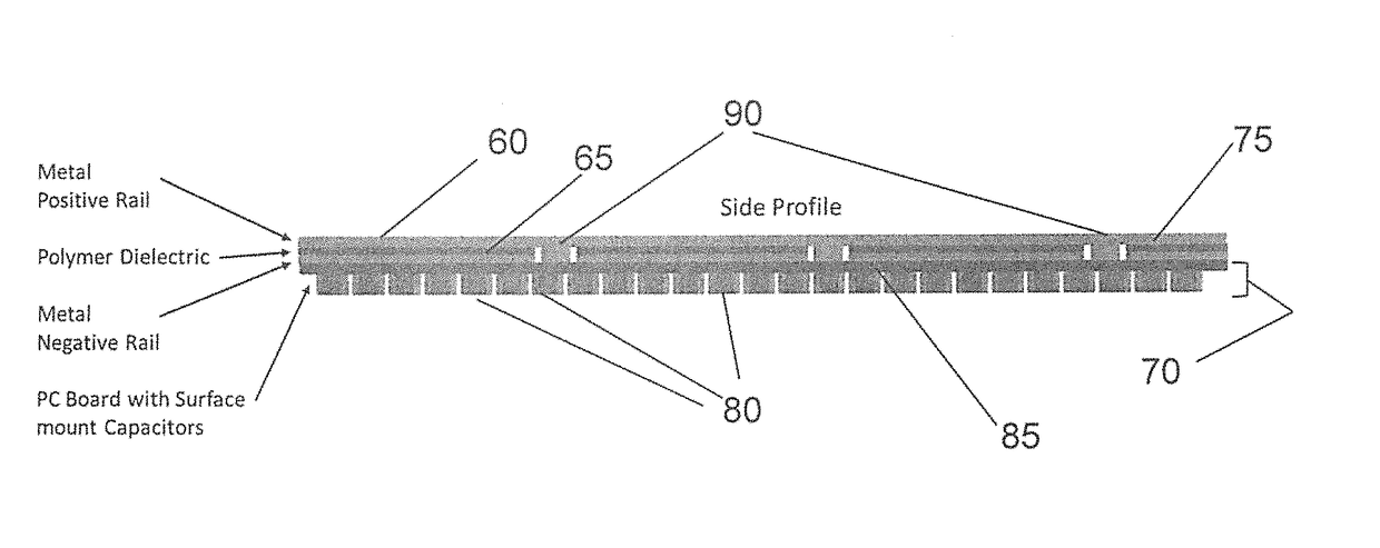
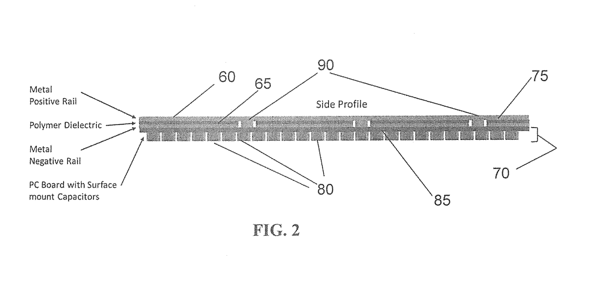
[0057]FIG. 3 is derived from a photographic image of the PCB used for our prototype. The PCB 95 was 6″×11″ in lateral dimensions, and it had a thickness of 0.062″. It had two conductive copper layers, with the required spacing between voltage potentials for avoidance of electrical breakdown. This was very important due to the high voltage and current levels present during operation.

[0058]An array of 336 MLCC capacitors 100 was connected in parallel to the PCB, providing a total nominal capacitance of 50.4 μF.

[0059]A multiple via-in-pad technique was used to connect the MLCCs to the PCB. This technique helped to minimize the loop inductance because it obviated the use of laterally extending conductors to make electrical connections.

[0060]The use of 2 oz. copper planes in the PCB facilitated heat dissipation and offered relatively low DC electrical resistance.

[0061]The bus plates, which matched the profile of the circuit board, were made of aluminum. As noted above, they serv...


PUM


Abstract

A DC power bus having reduced parasitic inductance and higher tolerable operating temperature is disclosed. In example embodiments, a bus structure overlies a printed circuit board, and an array of capacitors is arranged on a surface of the printed circuit board distal the bus structure. The bus structure comprises an upper metal plate, a lower metal plate, and a dielectric film interposed between the upper and lower metal plates. The capacitors are connected in parallel between conductive planes of the printed circuit board. The upper and lower metal plates of the bus structure are connected to respective conductive planes of the printed circuit board.

Description

CROSS-REFERENCE TO RELATED APPLICATION[0001]This application claims priority to U.S. Provisional Patent Application No. 62 / 292,473, filed on Feb. 8, 2016 under the title, “LOW-INDUCTANCE DIRECT CURRENT POWER BUS,” the entirety of which is hereby incorporated herein by reference.STATEMENT OF GOVERNMENT INTEREST[0002]This invention was made with Government support under contract no. DE-AC04-94AL85000 awarded by the U.S. Department of Energy to Sandia Corporation. The Government has certain rights in the invention.FIELD OF THE INVENTION[0003]The invention relates to electric power systems, and more particularly to systems that deliver DC power to or from power inverters. More particularly, the invention relates to power systems for electric vehicles, hybrid electric vehicles, solar photovoltaic power converters, and the like.Art Background[0004]The drive systems for electric vehicles (EVs) and hybrid electric vehicles (HEVs) must include circuitry to interconvert between the DC output ...

Claims


Application Information

Patent Timeline
IPC IPC(8): H01L23/34H02J1/02H01L29/16H02M7/00B60L11/18B60R16/03
CPCH02J1/02H01L29/1608H02M7/003B60L11/1803B60R16/03Y10S903/00H02J1/06Y02T10/92Y02E10/56Y02T10/70Y02T10/72
Inventor NEELY, JASON C.STEWART, JOSHUADELHOTAL, JAROD JAMESFLICKER, JACK DAVIDBRENNECKA, GEOFF L.
Owner NAT TECH & ENG SOLUTIONS OF SANDIA LLC
Why Eureka
Try Eureka