Supercharge Your Innovation With Domain-Expert AI Agents!

Wafer processing laminate and method for processing wafer

a wafer and processing laminate technology, applied in the direction of layered products, solid-state devices, semiconductor devices, etc., can solve the problems of inadequate strength and heat resistance, long treatment time per substrate, and tape is not suited to the steps, etc., to achieve convenient and convenient separation, excellent resistance to a wafer thermal process, and facilitate temporary adhesion

Active Publication Date: 2018-10-30
SHIN ETSU CHEM CO LTD
View PDF22 Cites 2 Cited by
  • Summary
  • Abstract
  • Description
  • Claims
  • Application Information

AI Technical Summary

Benefits of technology

The solution enables efficient and uniform processing of heavily stepped substrates with improved thermal resistance and easy separation of wafers, enhancing productivity and compatibility with various processes.

Problems solved by technology

However, this tape uses an organic resin film as its base, which has flexibility, but inadequate strength and heat resistance.
Thus, this tape is not suited to the steps of forming a TSV and forming a wiring layer on the back surface.
The former technique has problems, for example, a long treatment time per substrate.
The latter technique is simple because of control only by heat, but thermal stability is insufficient at a high temperature exceeding 200° C., and thus the applicable range is limited.
Furthermore, these temporary adhesive layers are not adequate to form a film with uniform thickness on a heavily stepped substrate and to completely adhere to the support.
Thus, this method takes a very long time for separation and is difficult to find application in the actual producing process.
In this method, however, the amount of the solvent that can be supplied to the adhesive is limited, and it takes a long time for separation.
Thus, this method is difficult to find application in the actual producing process.

Method used


Image

  • Wafer processing laminate and method for processing wafer
  • Wafer processing laminate and method for processing wafer
  • Wafer processing laminate and method for processing wafer

Examples


synthesis example 1

Resin Synthesis Example 1

[0187]A flask equipped with a stirrer, a thermometer, a nitrogen purge system, and a reflux condenser was charged with 43.1 g of 9,9′-bis(3-allyl-4-hydroxyphenyl)fluorene (M-1), 29.5 g of organohydrogensiloxane shown by the average structural formula (M-3), 135 g of toluene, and 0.04 g of chloroplatinic acid, and the mixture was heated at 80° C. Then, 17.5 g of 1,4-bis(dimethylsilyl)benzene (M-5) was added dropwise into the flask over 1 hour. At this time, the temperature inside the flask was increased to 85° C. After completion of dropwise addition, the mixture was aged at 80° C. for 2 hours, toluene was then distilled off, and 80 g of cyclohexanone was added thereto to obtain a resin solution (b1) containing cyclohexanone as a solvent with a concentration of the resin solid of 50 mass %. When the molecular weight of the resin in the solution was measured by GPC, the weight average molecular weight was 45,000 in terms of polystyrene.

synthesis example 2

Resin Synthesis Example 2

[0188]In a 5-L flask equipped with a stirrer, a thermometer, a nitrogen purge system, and a reflux condenser, 84.1 g of epoxy compound (M-2) was dissolved in 600 g of toluene. Then, 294.6 g of compound (M-3) and 25.5 g of compound (M-4) were added to the solution, and the mixture was heated at 60° C. Thereafter, 1 g of carbon carried platinum catalyst (5 mass %) was added thereto, and after confirming that the internal reaction temperature was increased to 65 to 67° C., the mixture was further heated to 90° C. and aged for 3 hours. Then, the mixture was cooled to room temperature, and 600 g of methyl isobutyl ketone (MIBK) was added thereto. This reaction solution was filtered under pressure through a filter to remove the platinum catalyst. The solvent in the resin solution was distilled off under reduced pressure, and 270 g of propylene glycol monomethyl ether acetate (PGMEA) was added thereto to obtain a resin solution (b2) containing PGMEA as a solvent wi...

synthesis example 3

Resin Synthesis Example 3

[0190]A four-necked flask was charged with 1,000 g (3.38 mol) of octamethylcyclotetrasiloxane and 0.93 g (0.003 mol) of tris(trimethylsiloxy)methylsilane, and the mixture was maintained at 110° C. Then, 4 g of 10 mass % tetrabutyl phosphonium hydroxide siliconate was added to the mixture. After polymerization over 4 hours, a post-treatment was carried out at 160° C. for 2 hours to obtain dimethylpolysiloxane.

[0191]The obtained dimethylpolysiloxane was analyzed by 29Si-NMR method to determine the ratio of D unit, M unit, and T unit, and consequently identified as a branched dimethylpolysiloxane having the following structure containing 99.911% of D unit, 0.067% of M unit, and 0.022% of T unit.

[0192]

[0193]500 g of the branched dimethylpolysiloxane was dissolved in 500 g of hexane, the solution was then added to 2 L of acetone, and the precipitated resin was collected. Thereafter, hexane, etc., were removed under vacuum to obtain a dimethylpolysiloxane polymer ...


PUM

PropertyMeasurementUnit
widthaaaaaaaaaa
peeling forceaaaaaaaaaa

Abstract

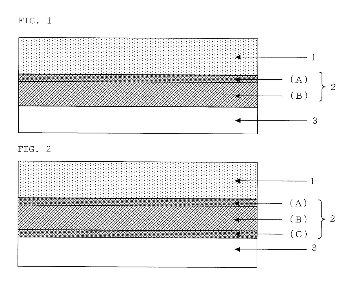
A wafer processing laminate including support, temporary adhesive material layer laminated on the support, and wafer stacked on temporary adhesive material layer, wafer having front surface on which circuit is formed and back surface to be processed, temporary adhesive material layer including first temporary adhesive layer composed of thermoplastic resin layer (A) laminated on front surface of wafer and second temporary adhesive layer composed of thermosetting resin layer (B) laminated on first temporary adhesive layer, thermoplastic resin layer (A) being soluble in cleaning liquid (D) after processing wafer, thermosetting resin layer (B) being insoluble in cleaning liquid (D) after heat curing and capable of absorbing cleaning liquid (D) such that cleaning liquid (D) permeates into layer (B). This wafer processing laminate allows a wide selection of materials, facilitates separation and collection of processed wafer, meets requirements on various processes, and can increase productivity of thin wafers.

Description

TECHNICAL FIELD[0001]The present invention relates to a wafer processing laminate and a method for processing a wafer which enable a thin wafer to be obtained effectively.BACKGROUND ART[0002]Three-dimensional semiconductor mounting has become essential for higher density and larger capacity. The three-dimensional mounting technique is a semiconductor production technique for thinning a semiconductor chip and connecting the chip to another chip by a through silicon via (TSV) to form a multilayer. To realize this technique, steps of grinding a non-circuit-forming surface (also referred to as “back surface”) of a substrate on which a semiconductor circuit has been formed to thin the substrate, and then forming an electrode including a TSV on the back surface, are required. In the step of grinding the back surface of a silicon substrate, a protective tape for the back surface is conventionally attached to a back side of the surface to be ground to prevent the wafer from breaking during ...

Claims


Application Information

Patent Timeline
Patent Type & Authority Patents(United States)
IPC IPC(8): H01L21/304B32B7/12C09J183/14C09J183/04B32B7/06H01L21/683C09J183/10C08G77/04C08G77/52C08G77/455
CPCH01L21/6836C09J183/04C09J183/10C09J183/14H01L21/304H01L21/6835H01L2221/68386C08G77/455C08G77/52H01L2221/6834H01L2221/68327H01L2221/68381C08G77/04H01L21/02008H01L21/02013H01L21/02016H01L21/568H01L21/76835H01L21/02052H01L21/76805H01L21/76832B32B7/12B32B7/06
Inventor TAGAMI, SHOHEISUGO, MICHIHIROKATO, HIDETO
Owner SHIN ETSU CHEM CO LTD
Features
  • R&D
  • Intellectual Property
  • Life Sciences
  • Materials
  • Tech Scout
  • Unparalleled Data Quality
  • Higher Quality Content
  • 60% Fewer Hallucinations
Learn More