Optical nanoprobing of integrated circuits

a technology of integrated circuits and optical nanoprobing, which is applied in the field of optoelectrical characterization of integrated circuits, can solve the problems of low spatial resolution, affecting the efficiency of photon collection, and running out of conventional far-field optical probing, which uses 1000-1500 nm lasers, etc., and achieves high spatial resolution.

Inactive Publication Date: 2019-01-08
FEI CO
View PDF3 Cites 0 Cited by
  • Summary
  • Abstract
  • Description
  • Claims
  • Application Information

AI Technical Summary

Benefits of technology

[0017]Aspects of the invention further include the following features: use of high transmission NFT (single or combination of more than one NFT) in OCA with resolution below diffraction limit; use of 3D nano motion transducer (example: piezo tube) to improve NFT's collection efficiency through optimizing angle and distance between the NFT and the sample surface; and, employment of efficient NFT's for fast high-resolution analysis of devices and circuits in frontside and backside nanoprobing.
[0023]According to another aspect a capability to deliver photons to the energized circuit with high spatial resolution is enabled.

Problems solved by technology

Conventional far-field optical probing, which uses 1000-1500 nm laser, is running out of resolution.
This solution has a serious limitation related to strong dependence of photon collection efficiency on the ratio of aperture diameter to wavelength (a fourth power dependence by Bethe's theory).
For practical applications photon collection efficiency is inadequate.
The problem with any near-field evanescence method is its poor photon delivery and collection efficiency.
This even further reduces the method's throughput and makes fiber NSOM-based high-resolution optical circuit analysis (OCA) simply impractical.
However, use of NSOM for collection of emitted or reflected photons is limited.
Considering sequential data collection algorithms of NSOM one faces a significant loss of throughput going from parallel imaging with 250 nm resolution to sequential scanning microscopy with 50 nm resolution (only extra data collection time can improve the signal-to-noise ratio, SNR).
Accordingly, there is a need in the art to enable probing of IC's at the upcoming design nodes, which cannot be probed using current technology due to insufficient resolution and / or photon collection efficiency.

Method used


Image

  • Optical nanoprobing of integrated circuits
  • Optical nanoprobing of integrated circuits
  • Optical nanoprobing of integrated circuits

Examples


Embodiment Construction

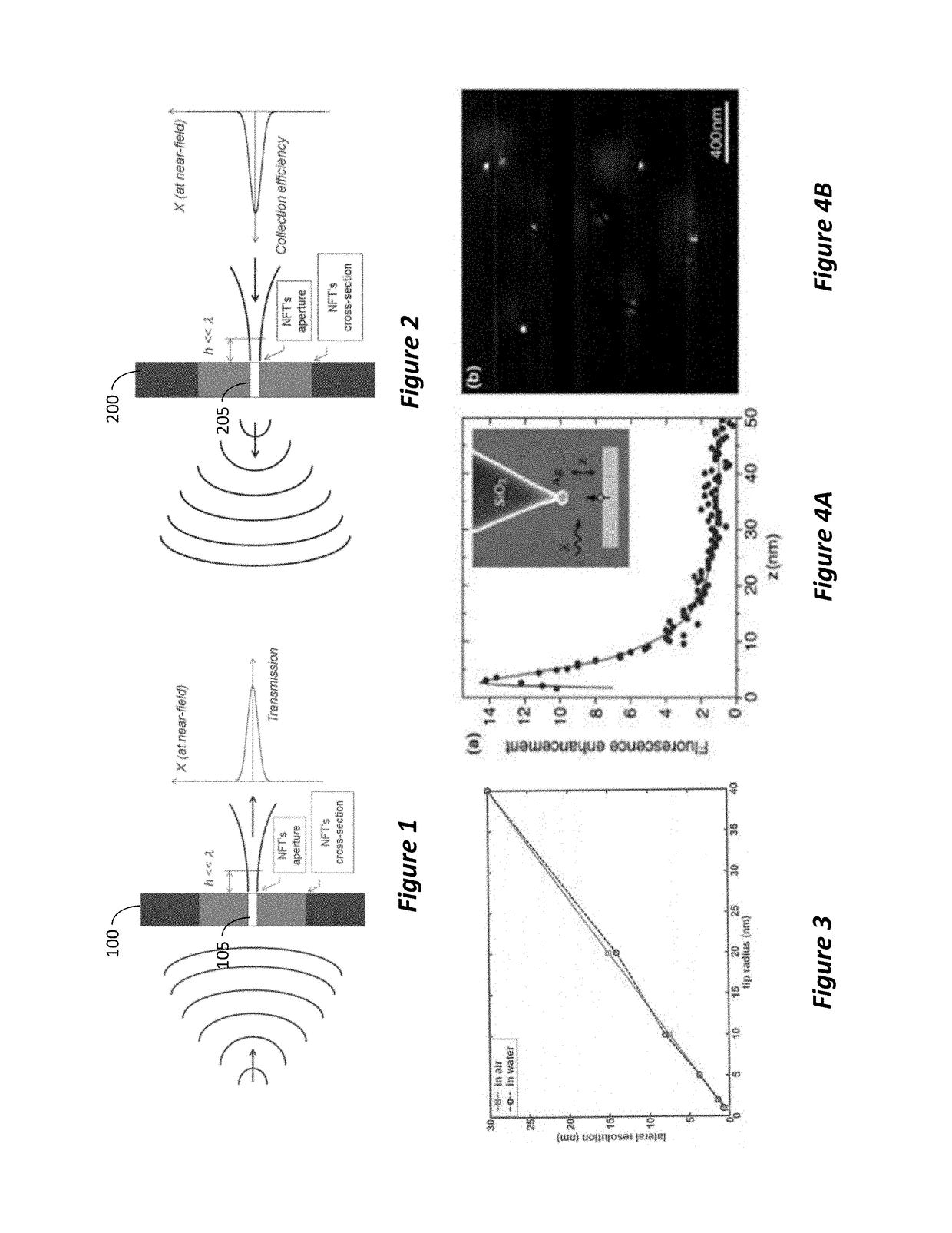
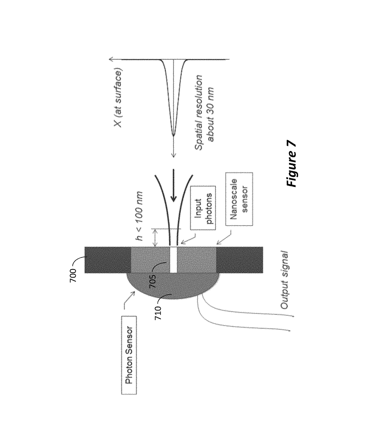
[0041]Relatively little is known about photon collection using NFT's. FIGS. 1 and 2 present illustrations of principals of both processes: photon delivery to the sample and collection of photons emitted by the sample, as implemented in disclosed embodiments.

[0042]FIG. 1 is an illustration of sub-wavelength focusing of light using NFT. Focused or plane wave (shown on the left) diffracts on plasmonic NFT 100 with effective cross-section of a few hundreds of nanometers. Intensified light penetrates to the right semi space through NFT's aperture 105, which defines dimensions of the focused beam in the near-field, wherein the aperture diameter is much smaller than the illumination wavelength and the object to be imaged is located a subwavelength distance from the aperture (h<<λ). Coupling efficiency or transmission of tens of percent can be achieved with NFT's. Light intensity of the focused beam may significantly (more than 100×) exceed the incident light intensity.

[0043]FIG. 2 is an il...


PUM

PropertyMeasurementUnit
diameteraaaaaaaaaa
heightaaaaaaaaaa
heightaaaaaaaaaa

Abstract

Apparatus for electrical and optical nanoprobing at resolution beyond optical diffraction limit. Navigation microscope is configured for navigation to a region of interest. A probe spatial positioner supports a fork and an oscillating piezotube is attached to the free end of the fork and provides an output indicating of a distance to the sample. A single-mode optical fiber having a near-field transducer formed at an end thereof is attached to the oscillating piezotube such that the near-field transducer extends below the oscillating piezotube towards the sample. A photodetector is positioned to detect photons collected from the sample. The near-field transducer may be formed as a tapered section formed at the end of the single-mode optical fiber, a metallic coating formed at a tip of the tapered section, and an aperture formed in the metallic coating so as to expose the tip of the tapered section through the metallic coating.

Description

CROSS-REFERENCE TO RELATED APPLICATIONS[0001]This application claims priority benefit from U.S. Provisional Patent Application, Ser. No. 62 / 184,822, filed on Jun. 25, 2015, the entire content of which is incorporated herein by reference.BACKGROUND[0002]1. Field of Invention[0003]This invention is in the field of optoelectrical characterization of integrated circuits (IC) using scanning or / and stepping (touching) nanoprobing systems.[0004]2. Related Art[0005]Nanoprobing covers a broad field of analytical science including various types of dimensional, electrical, mechanical, compositional and chemical physical characterization of nanoobjects. Nanoelectronic devices, such as advanced (<130 nm) ICs, are examples of such objects.[0006]Conventional far-field optical probing, which uses 1000-1500 nm laser, is running out of resolution. Currently even the most sophisticated photon delivery and collection optics (solid immersion lens SIL) provides lateral resolution of about 200 nm and w...

Claims


Application Information

Patent Timeline
Patent Type & Authority Patents(United States)
IPC IPC(8): G01N21/65G01R31/311
CPCG01R31/311Y10S977/901G01N21/658G01R31/2886G01N29/2437G01N29/2418G01N29/2462
Inventor UKRAINTSEV, VLADIMIR A.BERKMYRE, MIKE
Owner FEI CO
Why Eureka
Try Eureka