Advanced thermally compensated surface acoustic wave device and fabrication

a surface acoustic wave and thermal compensation technology, applied in the manufacture/assembly of piezoelectric/electrostrictive devices, impedence networks, electrical devices, etc., can solve the problems of delamination of metalized parts, wafer breakage, and limited approach, and achieve the effect of low insertion loss

Active Publication Date: 2019-04-23
SOITEC SA
View PDF22 Cites 0 Cited by
  • Summary
  • Abstract
  • Description
  • Claims
  • Application Information

AI Technical Summary

Benefits of technology

[0009]This method of fabrication has the advantage that the dielectric structure can be provided in a separate process to the providing of the piezoelectric structure and, thus, certain incompatibilities can be avoided. For instance, one is no longer limited to dielectric materials suitable for deposition on a piezoelectric material but has a much larger choice. Further, as the metallization is performed on the dielectric structure and not the inverse, dielectric materials sustaining high formation temperature may be used, such as, for instance, thermally grown silicon oxide, because there is no risk of diffusion of metal as it is formed in an ulterior step. Such high quality dielectric materials also allow a much better control of the metallization and, in particular, a much better control of the interface between the dielectric structure and the metalized parts, thus avoiding parasitic effects causing perturbation of the surface acoustic waves. Further, to the mentioned advantages, the thermal compensation of the surface acoustic wave device allowing a much higher thermal stability of its frequency response is obtained due to the stiffening provided by the dielectric structure and its counteracting TCE.
[0043]This provides the beneficial advantage that the surface acoustic wave device can be used for high power applications, together with very low insertion losses.

Problems solved by technology

However, this approach is rather limited for several reasons.
In addition, the rather high TCE of the commonly used piezoelectric substrates 100 can further cause manufacturing problems due to warping or bending or induced strain if several materials with different TCE are in contact with each other and the temperatures applied exceed the maximal tolerated limit, as may be the case for the metallization 110 formed on top of the piezoelectric substrate 100, and the thermal budget employed during the formation of the dielectric layer 120 may lead to delamination of the metalized parts 110 or even breakage of the wafer.
Further, the formation of the dielectric layer 120 at rather low temperatures, as can be the case for certain amorphous SiO2 layers, leads to rather low quality material with reduced acoustic properties and, thus, limits the performance of SAW technology based on it.
Even further, unavoidable growth defects due to the deposition of the dielectric layer 120 on both the metalized parts 110 and the piezoelectric substrate 100, together with the fact that the metalized parts 110 comprise horizontal and vertical parts with respect to the growth direction of the dielectric layer 120, lead to parasitic electro-acoustic effects, especially at the intersections of the vertical and horizontal parts and, thus, losses of performance of the SAW device 10.

Method used


Image

  • Advanced thermally compensated surface acoustic wave device and fabrication
  • Advanced thermally compensated surface acoustic wave device and fabrication
  • Advanced thermally compensated surface acoustic wave device and fabrication

Examples


Embodiment Construction

[0048]This disclosure will now be described with reference to specific embodiments. It will be apparent to the skilled person that features and alternatives from any of the embodiments can be combined, independently of each other, with features and alternatives of any other embodiment in accordance with the scope of the claims.

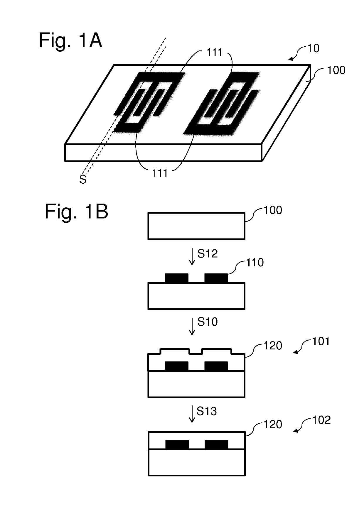
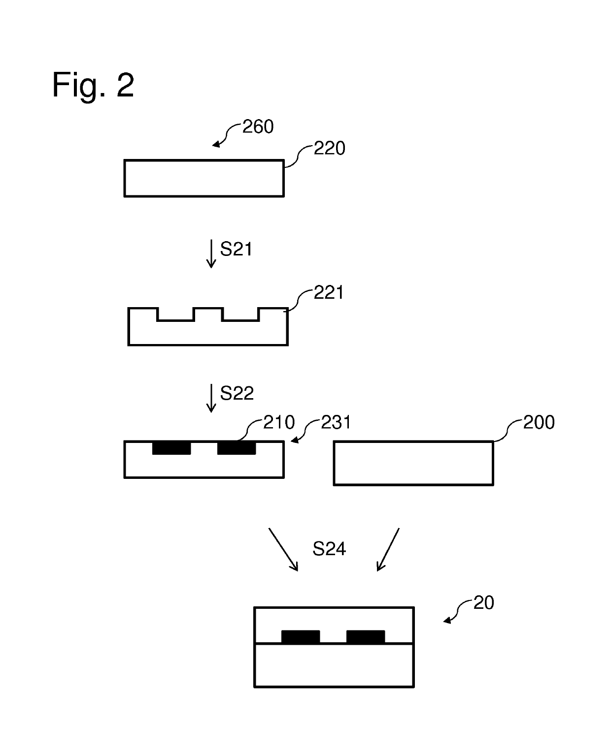
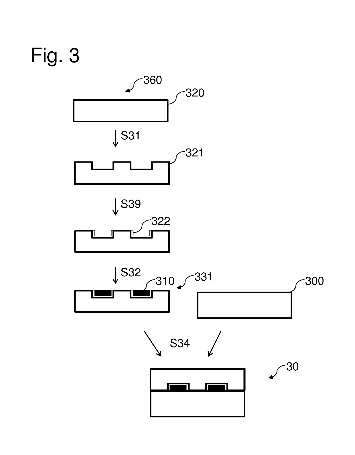
[0049]FIG. 2 schematically shows a fabrication method of a SAW device 20 in accordance with embodiments of this disclosure. An etching step S21 is performed on a dielectric structure 260 comprising a dielectric layer 220, which results in an etched dielectric layer 221 including etched and non-etched parts. A subsequent metallization step S22 is performed to fill up in a flush manner the etched parts of the etched dielectric layer 221 with metalized parts 210, resulting in a metalized dielectric layer structure 231 comprising a dielectric layer 220 comprising electrically conductive means, in particular, metalized parts 210. After the formation of the metalize...


PUM


Abstract

This disclosure relates to a method of fabrication of a surface acoustic wave device comprising the step (a) of providing a piezoelectric structure, the step (b) of providing a dielectric structure, wherein the step (b) comprises a step (b1) of metalizing the dielectric structure, and the method further comprising the step (c) of bonding the metalized dielectric structure to the piezoelectric structure.

Description

CROSS-REFERENCE TO RELATED APPLICATIONS[0001]This application is a national phase entry under 35 U.S.C. § 371 of International Patent Application PCT / EP2014 / 055746, filed Mar. 21, 2014, designating the United States of America and published in English as International Patent Publication WO 2014 / 166722 A1 on Oct. 16, 2014, which claims the benefit under Article 8 of the Patent Cooperation Treaty and under 35 U.S.C. § 119(e) to French Patent Application Serial No. 13 / 00824, filed Apr. 8, 2013, the disclosure of each of which is hereby incorporated herein in its entirety by this reference.TECHNICAL FIELD[0002]This disclosure relates to a method of fabrication of a surface acoustic wave device and to a surface acoustic wave device.BACKGROUND[0003]Acoustic resonator structures such as surface acoustic wave (SAW) devices 10 use one or more interdigitated transducers (IDTs) 111 provided on a piezoelectric substrate 100 to convert electrical signals to acoustic waves and vice versa, as sche...

Claims


Application Information

Patent Timeline
Patent Type & Authority Patents(United States)
IPC IPC(8): H01L41/22H03H9/25H03H3/08
CPCH03H3/08H03H9/25
Inventor ZINKE, CHRISTOPHEDESBONNETS, ERIC
Owner SOITEC SA
Why Eureka
Try Eureka