Silicon-on-insulator device and intermetallic dielectric layer structure thereof and manufacturing method

a technology of silicon-on-insulator and intermetallic dielectric layer, which is applied in the direction of semiconductor devices, semiconductor/solid-state device details, electrical apparatus, etc., can solve the problems of failure of goi, gate oxide (gox), junction or poly edge, and inability to discharge mobile ions, so as to avoid the damage of the device by accumulation of mobile ions at the interface. , good performance

Active Publication Date: 2019-04-30
CSMC TECH FAB2 CO LTD
View PDF14 Cites 0 Cited by
  • Summary
  • Abstract
  • Description
  • Claims
  • Application Information

AI Technical Summary

Benefits of technology

[0016]For the above SOI device, when the mobile ions generated during the back end process move towards the lower structures through the Si-rich oxide layer, the Si-rich oxide layer with greater thickness can capture and bind the mobile ions to the unsaturated bond, such that it is difficult for the mobile ions to pass through the Si-rich oxide layer, and the purpose of blocking the mobile ions is achieved. Therefore, the device exhibits a good performance in evaluation of gate oxide integrity (GOI), and the damage of the device by accumulation of the mobile ions at the interface is avoided.

Problems solved by technology

However, for the SOI process, due to presence of buried layer oxidation, the mobile ions cannot be discharged.
Therefore, the device can be influenced obviously, which may easily cause disadvantages of gate oxide (GOX), junction or Poly edge.
In evaluation of gate oxide layer integrity (GOI), GOI fail occurs.

Method used


Image

  • Silicon-on-insulator device and intermetallic dielectric layer structure thereof and manufacturing method
  • Silicon-on-insulator device and intermetallic dielectric layer structure thereof and manufacturing method
  • Silicon-on-insulator device and intermetallic dielectric layer structure thereof and manufacturing method

Examples


Embodiment Construction

[0020]The objects, features and advantages of the present invention will become more apparent by describing in detail embodiments thereof with reference to the accompanying drawings.

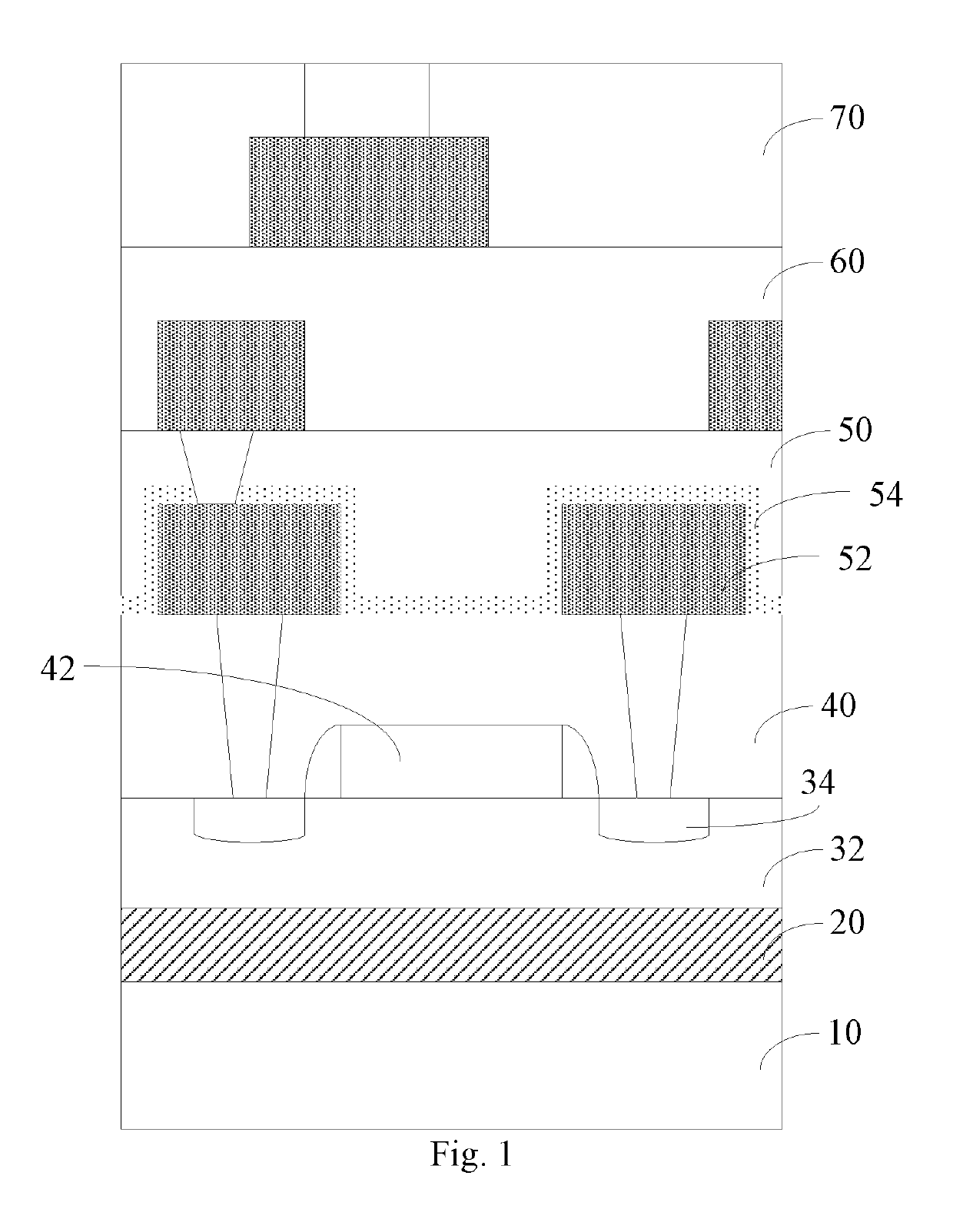
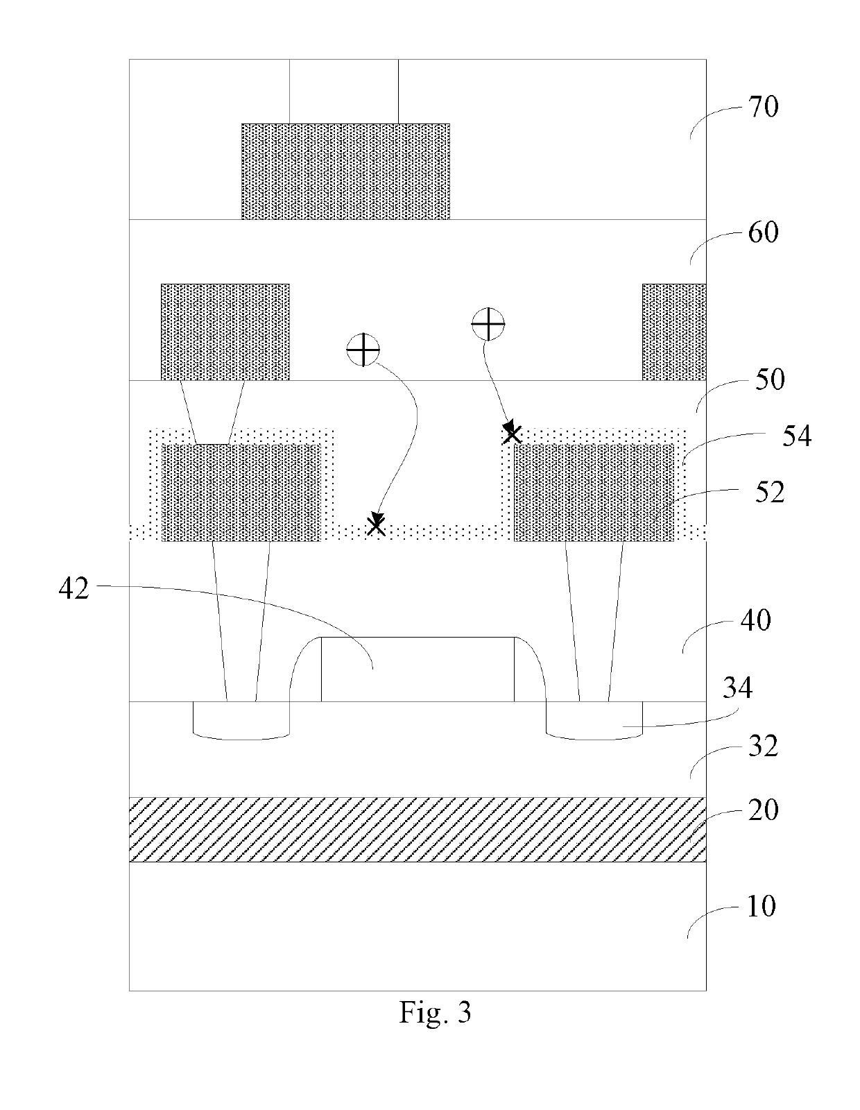
[0021]FIG. 1 is a sectional view of the silicon-on-insulator (SOI) device in an embodiment. The device includes a substrate 10, a buried oxide layer 20 formed on the substrate 10, a well region 32 formed on the buried oxide layer 20, a source (drain) structure 34 formed in the well region 32, a gate oxide layer (not shown in FIG. 1), a gate 42 and an interlayer dielectric (ILD) layer 40 formed on the well region 32, a first intermetallic dielectric layer 50 formed on the interlayer dielectric layer 40 and a pad layer 70 formed on a surface of the device. In the embodiment, a silicon oxide layer is included in the interlayer dielectric layer 40. One or more second intermetallic dielectric layers 60 may be also provided between the first intermetallic dielectric layer 50 and the pad layer 70. The first int...


PUM

PropertyMeasurementUnit
thicknessaaaaaaaaaa
thicknessaaaaaaaaaa
thicknessaaaaaaaaaa

Abstract

Provided is an intermetallic dielectric layer structure of a silicon-on-insulator device, comprising a silicon-rich oxide layer (54) covering a metal interconnect, a fluorine-silicon glass layer on the silicon-rich oxide layer, and a non-doped silicate glass layer on the fluorine-silicon glass layer; the thickness of the silicon-rich oxide layer (54) is 700 angstroms .+-.10%; the silicon-rich oxide layer having a greater thickness captures movable ions on an unsaturated bond, such that it is difficult for the movable ions to pass through the silicon-rich oxide layer, thus blocking the movable ions. The present invention has good performance in an integrity evaluation of the gate oxide layer, and avoids damage to the device caused by the aggregation of movable ions at an interface. Also provided are a silicon-on-insulator device and a method of manufacturing the intermetallic dielectric layer of the silicon-on-insulator device.

Description

FIELD OF THE INVENTION[0001]The present invention relates to semiconductor devices, and particularly relates to an intermetallic dielectric layer structure of a silicon-on-insulator device, a device having the intermetallic dielectric layer structure, and a method of manufacturing an intermetallic dielectric layer of the silicon-on-insulator device.BACKGROUND OF THE INVENTION[0002]In a conventional 0.18 micron logic 1.8V / 3.3V silicon-on-insulator (SOI) process, a 0.18 micron logic process is usually used in the back end process. However, through experimental study, the inventor finds that a larger number of mobile ions are generated during the back end process. These mobile ions can conduct along the metal lead, the via, and the intermetallic film, and accumulate at the Si—SiO2 interface, the polysilicon (Poly) edge and the like, which influences the interface state. For the ordinary bulk silicon process, these mobile ions can be discharged out of the substrate, such that the accumu...

Claims


Application Information

Patent Timeline
Patent Type & Authority Patents(United States)
IPC IPC(8): H01L21/768H01L23/532H01L27/12H01L21/02H01L23/528
CPCH01L21/76834H01L21/02131H01L21/02164H01L21/02274H01L21/76801H01L23/5283H01L23/53295H01L27/1248H01L2924/0002H01L2924/00
Inventor WANG, ZHIYONGWANG, DEJINMA, JINGJING
Owner CSMC TECH FAB2 CO LTD
Why Eureka
Try Eureka