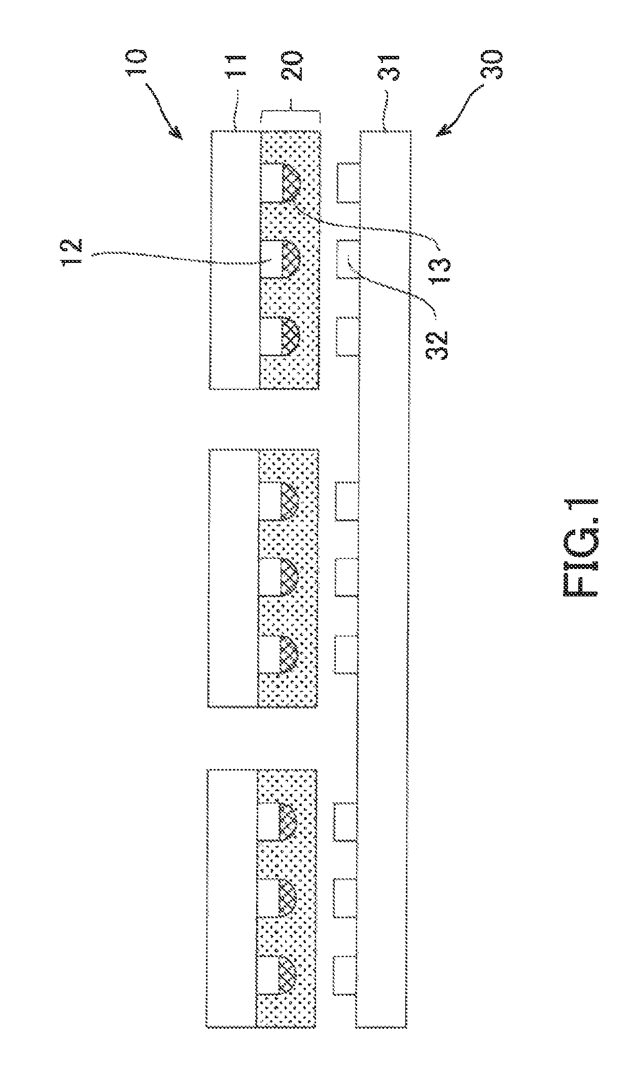
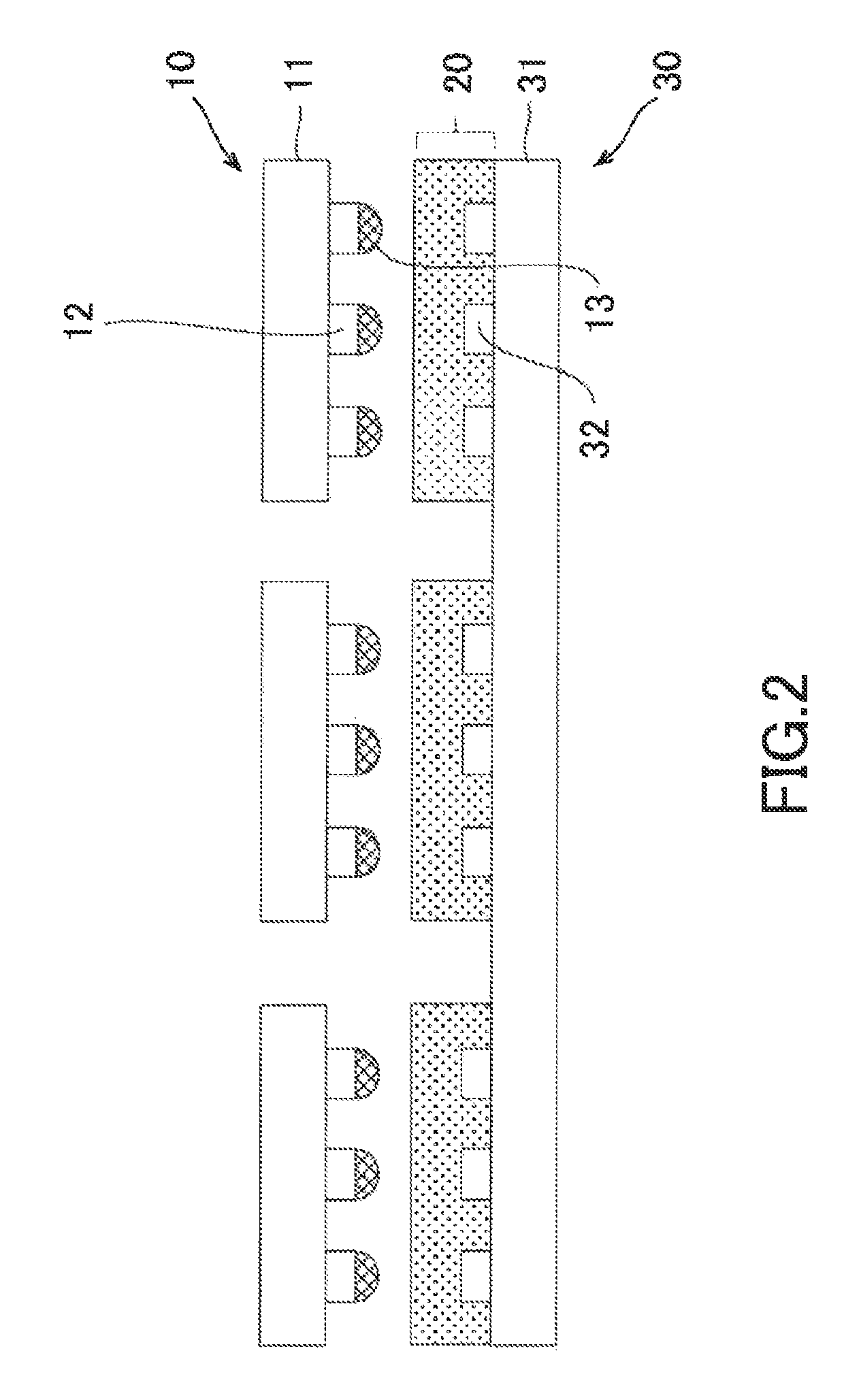
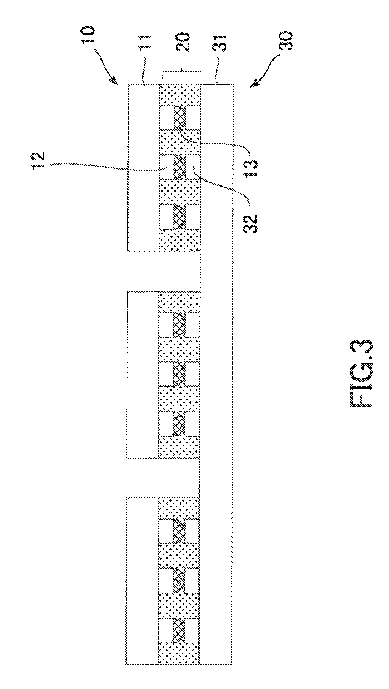
Semiconductor device manufacturing method and underfill film
a semiconductor and manufacturing method technology, applied in the direction of film/foil adhesives without carriers, semiconductor/solid-state device details, film/foil adhesives, etc., can solve the problems of increasing the cost of per chip, difficulty in mounting thin semiconductor chips and 3d mounting with conventional liquid underfill film materials, and high cost of multi-head devices, so as to reduce the effect of chip-position-dependent temperature-increase differences and excellent solder bonding properties
- Summary
- Abstract
- Description
- Claims
- Application Information
AI Technical Summary
Benefits of technology
Problems solved by technology
Method used
Image

Examples
reference example 1
[0086]A 70 / 30 acrylic / epoxy resin composition was prepared by blending 40 pts. mass of an acrylic rubber polymer (Teisan Resin SG-P3, Nagase ChemteX Corporation) as a film forming resin, 20 pts. mass of an epoxy (JER1031S, Mitsubishi Chemical Corporation), 10 pts. mass of acid anhydride (RIKACID HNA-100, New Japan Chemical Co. Ltd.), 1 pt. mass of an imidazole as a curing accelerator (U-CAT-5002, San-Apro Co. Ltd.), 68 pts. mass of an acrylic resin (OGSOL EA-0200, OSAKA ORGANIC CHEMICAL INDUSTRY LTD.), 2 pts. mass of an organic peroxide (PERHEXA V, NOF CORPORATION), and 15 pts. mass of a filler (AEROSIL R202, NIPPON AEROSIL CO. LTD.). This was coated to release treated PET (polyethylene terephthalate) using a bar coater and dried in an oven at 80° C. for 3 minutes to prepare an underfill film having a thickness of 50 μm (cover release-treated PET (25 μm) / underfill film (50 μm) / base release-treated PET (50 μm).
[0087]Melt viscosity curves of Reference Example 1 are shown in FIG. 13. E...
reference example 2
[0088]A 50 / 50 acrylic / epoxy resin composition was prepared by blending 40 pts. mass of an acrylic rubber polymer (Teisan Resin SG-P3, Nagase ChemteX Corporation) as a film forming resin, 30 pts. mass of an epoxy (JER1031S, Mitsubishi Chemical Corporation), 20 pts. mass of acid anhydride (RIKACID HNA-100, New Japan Chemical Co. Ltd.), 1 pt. mass of an imidazole as a curing accelerator (U-CAT-5002, San-Apro Co. Ltd.), 49 pts. mass of an acrylic resin (OGSOL EA-0200, OSAKA ORGANIC CHEMICAL INDUSTRY LTD.), 1 pt. mass of an organic peroxide (PERHEXA V, NOF CORPORATION), and 15 pts. mass of a filler (AEROSIL R202, NIPPON AEROSIL CO. LTD.). This was coated to release treated PET (polyethylene terephthalate) using a bar coater and dried in an oven at 80° C. for 3 minutes to prepare an underfill film having a thickness of 50 μm (cover release-treated PET (25 μm) / underfill film (50 μm) / base release-treated PET (50 μm).
[0089]Melt viscosity curves of Reference Example 2 are shown in FIG. 13. Ev...
reference example 3
[0090]A 50 / 50 acrylic / epoxy resin composition was prepared by blending 40 pts. mass of an acrylic rubber polymer (Teisan Resin SG-P3, Nagase ChemteX Corporation) as a film forming resin, 45 pts. mass of an epoxy (JER1031S, Mitsubishi Chemical Corporation), 15 pts. mass of acid anhydride (RIKACID HNA-100, New Japan Chemical Co. Ltd.), 1 pt. mass of an imidazole as a curing accelerator (U-CAT-5002, San-Apro Co. Ltd.), 39 pts. mass of an acrylic resin (OGSOL EA-0200, OSAKA ORGANIC CHEMICAL INDUSTRY LTD.), 1 pt. mass of an organic peroxide (PERHEXA V, NOF CORPORATION), and 15 pts. mass of a filler (AEROSIL R202, NIPPON AEROSIL CO. LTD.). This was coated to release treated PET (polyethylene terephthalate) using a bar coater and dried in an oven at 80° C. for 3 minutes to prepare an underfill film having a thickness of 50 μm (cover release-treated PET (25 μm) / underfill film (50 μm) / base release-treated PET (50 μm).
[0091]Melt viscosity curves of Reference Example 3 are shown in FIG. 13. Ev...
PUM
| Property | Measurement | Unit |
|---|---|---|
| temperature | aaaaa | aaaaa |
| temperature | aaaaa | aaaaa |
| temperature | aaaaa | aaaaa |
Abstract
Description
Claims
Application Information
 - R&D
- Intellectual Property
- Life Sciences
- Materials
- Tech Scout
- Unparalleled Data Quality
- Higher Quality Content
- 60% Fewer Hallucinations
Browse by: Latest US Patents, China's latest patents, Technical Efficacy Thesaurus, Application Domain, Technology Topic, Popular Technical Reports.
© 2025 PatSnap. All rights reserved.Legal|Privacy policy|Modern Slavery Act Transparency Statement|Sitemap|About US| Contact US: help@patsnap.com