Printed circuit board and method of manufacturing the same

a technology of printed circuit boards and printed circuits, applied in the direction of conductive pattern formation, conductive element electric connection formation, insulating substrate metal adhesion improvement, etc., can solve the problem of difficult fine pitch formation, and achieve the effect of minimizing the difference due to thermal shock and maximizing the adhesion between the circuit pattern and the insulating resin

Active Publication Date: 2019-05-07
LG INNOTEK CO LTD
View PDF7 Cites 0 Cited by
  • Summary
  • Abstract
  • Description
  • Claims
  • Application Information

AI Technical Summary

Benefits of technology

[0009]The embodiment provides a PCB capable of improving a bonding force between a substrate and a metal layer by forming a circuit pattern on a metal layer including a nitride as a seed layer and a method of manufacturing the same.
[0030]According to the embodiment, in order to form a fine pattern, the adhesion force of a circuit pattern even in a narrow area is required to be maximized. By forming the circuit pattern based on the metal layer including a nitride, the adhesion between the circuit pattern and the insulating resin can be maximized without a separate surface roughness treatment process.
[0031]In addition, according to the embodiment, the difference due to a thermal shock can be minimized as the deviation between the metal seed layer and the insulating resin layer is reduced due to a difference in thermal expansion coefficients.

Problems solved by technology

If the thickness of the seed layer is thick, the lead time of a flesh etching process for removing the seed layer becomes long and it is difficult to form a fine pitch.

Method used


Image

  • Printed circuit board and method of manufacturing the same
  • Printed circuit board and method of manufacturing the same
  • Printed circuit board and method of manufacturing the same

Examples


Embodiment Construction

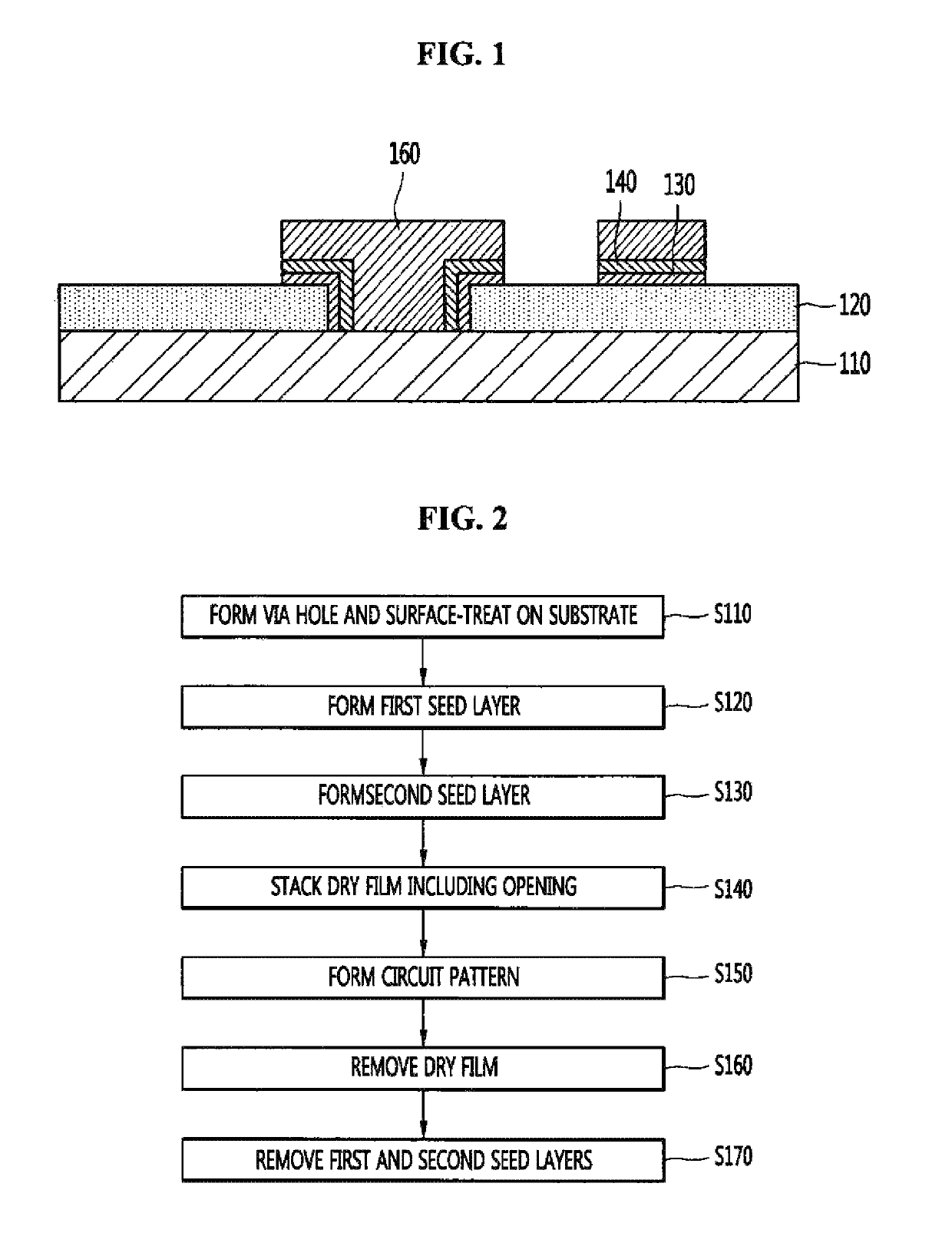
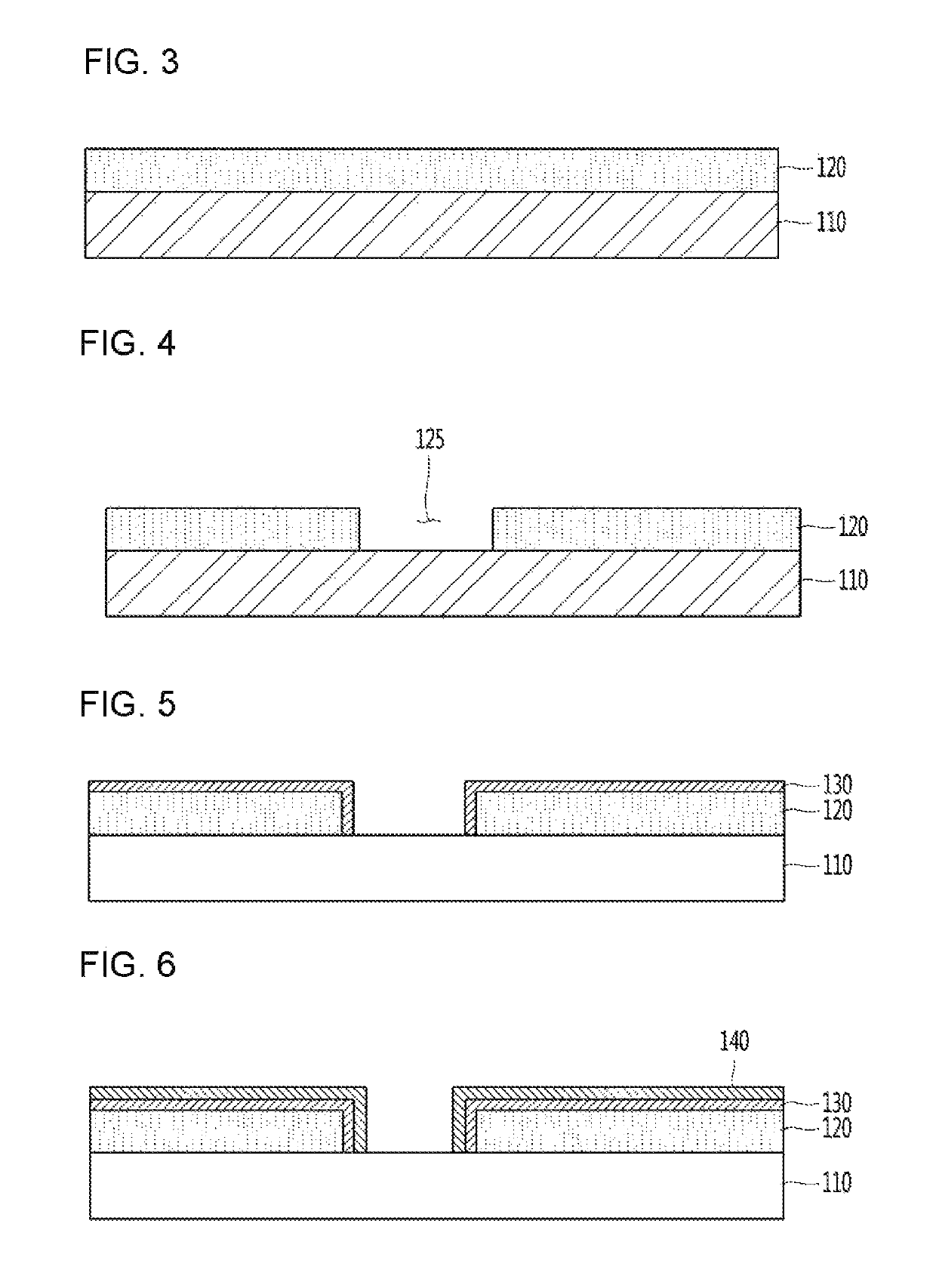
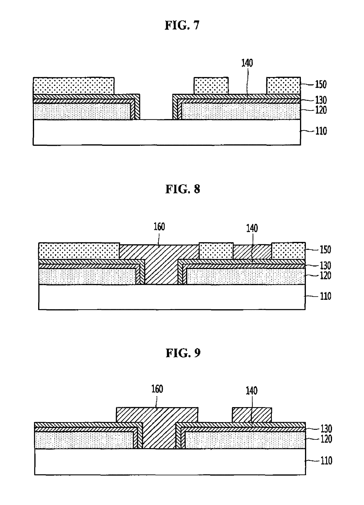
[0037]Hereinafter, exemplary embodiments of the present invention that are easily performed by those skilled in the art will be described in detail with reference to the accompanying drawings. However, the present invention may be implemented in various different forms and is not limited to the embodiments described herein.

[0038]In the following description, when there is an expression that some portion “includes” some structural elements, this means that some portion does not exclude another structural element, but may further include another structural element unless stated to the contrary.

[0039]Further, structures and elements which do not relate to the detail description are not shown in the drawings to clearly describe the present invention, thicknesses may be exaggerated to clearly explain various layers and regions, and similar elements in the following description are designated by similar reference numerals.

[0040]It will be understood that when a portion of a layer, a film,...


PUM


Abstract

A printed circuit board (PCB) includes: a substrate; and a circuit pattern disposed on the substrate, wherein the circuit pattern includes a first seed layer disposed on the substrate and including a nitride, and a metal layer disposed on the first seed layer.

Description

CROSS-REFERENCE TO RELATED APPLICATION(S)[0001]The present application claims priority under 35 U.S.C. 119 and 35 U.S.C. 365 to Korean Patent Application No. 10-2016-0065589, filed on May 27, 2016, which is hereby incorporated by reference in its entirety.BACKGROUND[0002]1. Field of the Invention[0003]The embodiment relates to a printed circuit board (PCB), and more particularly, to a PCB including a circuit pattern formed of a seed layer of a nitride metal layer and a method of manufacturing the same.[0004]2. Description of Related Art[0005]Recently, as a substrate serving as an interposer between a substrate and an electronic device has rapidly become light and thin, a high density and a fine pattern have been demanded. Various efforts have been made to shorten an existing process as well as improvement of technology.[0006]An additive method is used for forming a circuit pattern of a PCB. The additive method forms the circuit pattern on an insulating layer by a plating method. Rec...

Claims


Application Information

Patent Timeline
Patent Type & Authority Patents(United States)
IPC IPC(8): H05K1/09H05K3/42H05K3/40H05K3/00H05K1/11H05K3/38H05K3/46H05K1/03H05K3/10
CPCH05K1/09H05K1/112H05K1/115H05K3/0011H05K3/388H05K3/4038H05K3/422H05K3/4644H05K1/0353H05K2201/09509H05K1/11H05K3/108H05K3/4069H05K3/4076H05K3/423H05K3/38H05K3/188H05K3/281H05K3/381H05K3/421
Inventor PARK, GI GON
Owner LG INNOTEK CO LTD
Why Eureka
Try Eureka