Integrated circuit verification using parameterized configuration

a technology of integrated circuit and configuration, applied in the direction of logic circuit, digital circuit testing, electronic circuit testing, etc., can solve the problems of large silicon ic re-spins, large fraction of silicon ic re-spins, and large fraction of debugging efforts

Inactive Publication Date: 2019-05-21
UNIV GENT
View PDF27 Cites 1 Cited by
  • Summary
  • Abstract
  • Description
  • Claims
  • Application Information

AI Technical Summary

Benefits of technology

[0012]It is an object of embodiments of the present invention to provide good means and methods for debugging and verifying an FPGA design or an ASIC design implemented in a FPGA.
[0013]It is an advantage of embodiments of the present invention that a short debugging cycle can be achieved.
[0014]It is an advantage of embodiments of the present invention that a high degree of signal visibility can be achieved while debugging a hardware design or ASIC design emulation on a FPGA platform.

Problems solved by technology

Verifying the correct operation within time-to-market constraints can be a challenge for ASIC design teams.
For example, 35 to 45 percent of the total ASIC development effort may be spent on verification, and this fraction may continue to grow due to the constant increase of chip complexity.
Moreover, debugging may consume about 60 percent of the total verification effort and may be the fastest growing component.
For example, a large fraction of silicon IC re-spins may be at least partially due to functional errors and bugs inadvertently introduced at the register-transfer level (RTL) stage of the design process.
Embedded systems are becoming even more complex.
Errors in the specification, the design and the implementation may be substantially unavoidable.
Efficient verification tools for verifying designs are therefore important, and even more so for ASIC designs, where errors cannot be easily fixed.
In addition, a late introduction of the product can invoke an important loss of revenues.
Thus, application specific integrated circuit (ASIC) verification and debugging has become a challenging and time consuming task in ASIC design, particularly because state of the art ASIC designs can be quite large and complex.
However, the inefficiency of software simulation and timing constraints can prohibit the debugging of complete systems through software simulation.
Moreover, the complexity of integrated circuits continues to increase, consistent with Moore's Law.
However, due to the inherent reconfigurability of static RAM-based FPGAs (SRAM-FPGAs), this implementation can also be performed on the fly, e.g. by run-time hardware generation.
Unfortunately, state of the art methods for hardware generation can be computationally expensive, such that run-time hardware generation may not be feasible for most applications given realistic time constraints.
However, FPGA emulation can suffer from a lack of on-chip signal observability and a lengthy recompilation cycle.
Observability of the internal signals can be enhanced by instrumentation of the design, but only a limited amount of such instruments can be inserted due to resource constraints.
The monitored subset can be changed by a recompilation, but each instrument-compile-debug iteration can take multiple hours due to this time-consuming recompilation.
This severely limits debug productivity and may result in a slow time-to-market.
Such trace-buffer IP can be inserted but require additional area and therefor are limited in number as such additional area is not always available (large designs may use the entire FPGA area).
However, such approach as known in the art may have the disadvantage of requiring signal predetermination and full recompilation.
However, in this approach signal predetermination is also required and run time flexibility via parameterized configuration is not provided.
However, this may have the disadvantage of requiring the selection of a set of signals for observation before any bugs are known is required.
The solutions such as a multiplexer network also require a lot of extra resources on the FPGA, increasing the used area.
Some tools as known in the art may however support a limited amount of reconfiguration.
Nevertheless, even though it may be possible to modify the trigger conditions during runtime, changing the signals under observation does require a lengthy FPGA recompilation, even with the more advanced techniques known in the art.
However, in typical realistic designs, few available resources are left for the Virtual Overlay Network and the Virtual Overlay Network thus typically may be too small.
Thus, insertion of extra instrumentation in the free multiplexers can be impractical in FPGA emulation of a large ASIC design.

Method used


Image

  • Integrated circuit verification using parameterized configuration
  • Integrated circuit verification using parameterized configuration
  • Integrated circuit verification using parameterized configuration

Examples


Embodiment Construction

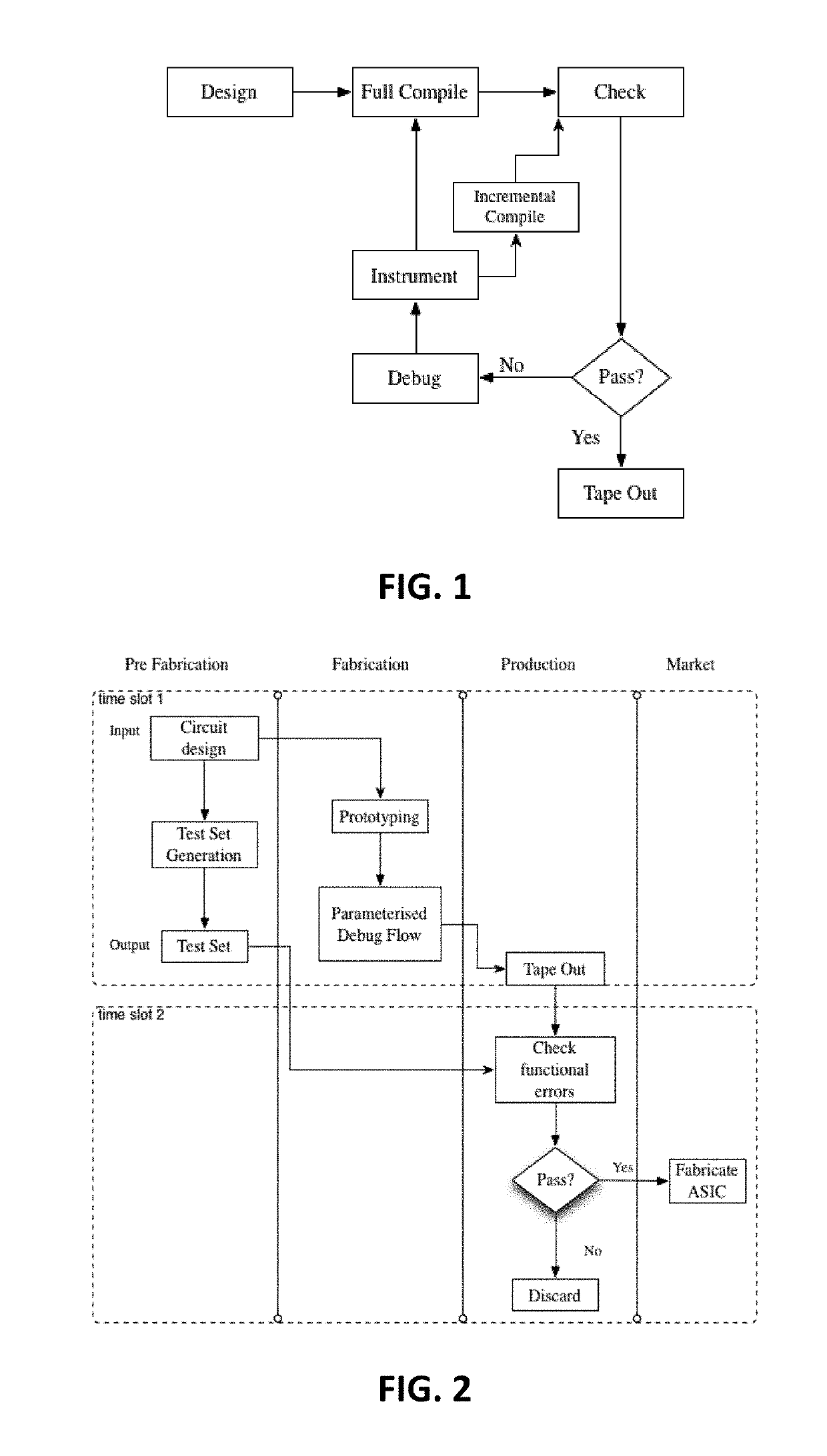
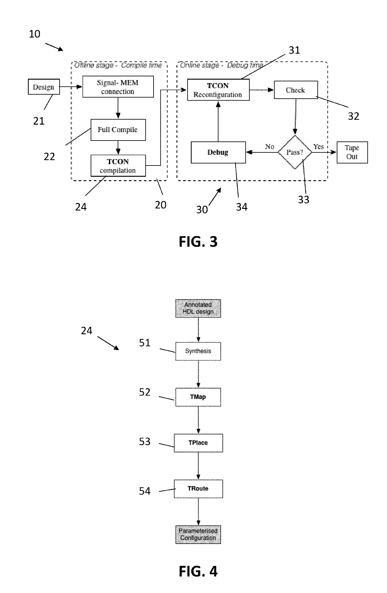
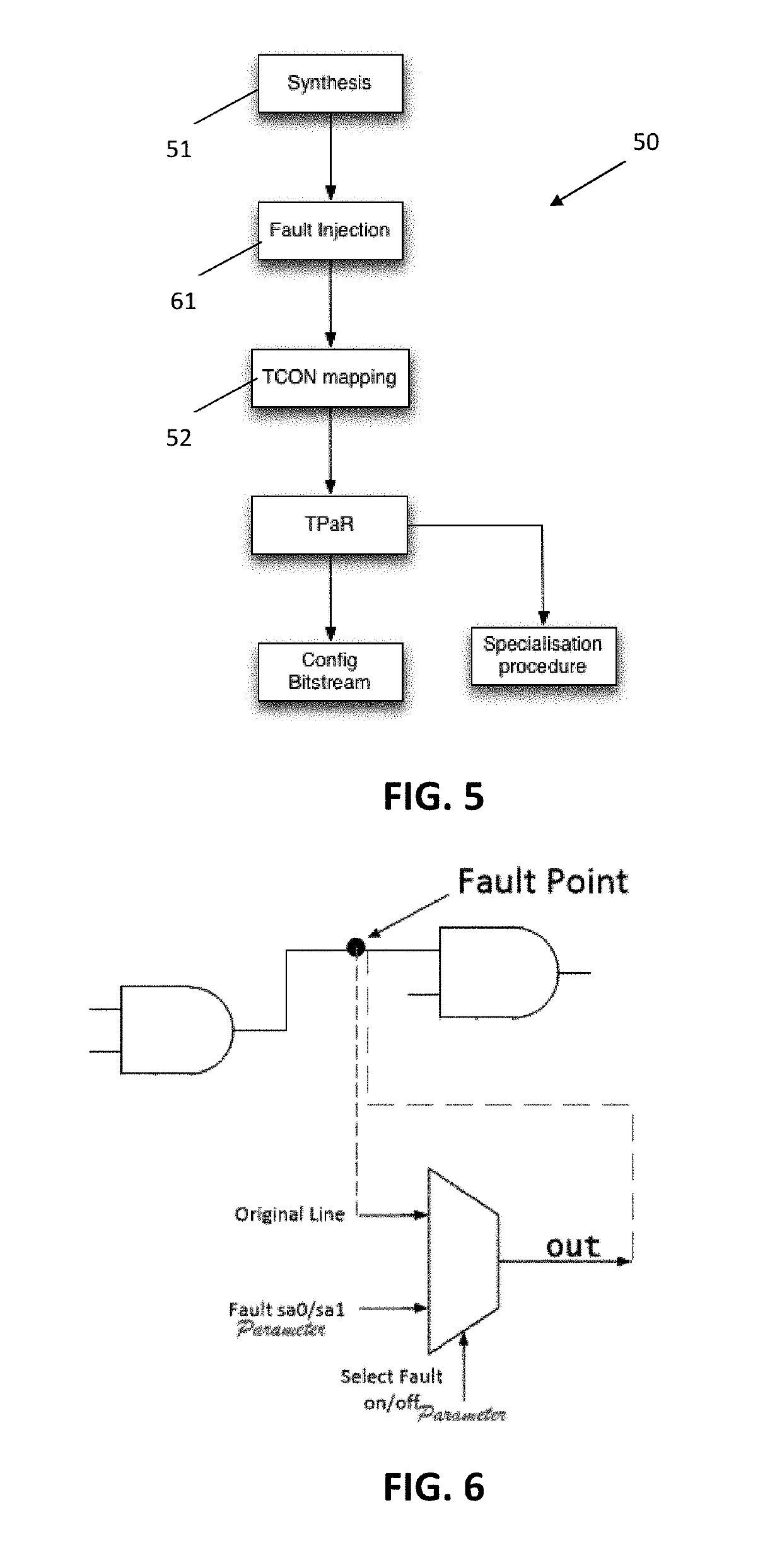
[0065]The present invention will be described with respect to particular embodiments and with reference to certain drawings but the invention is not limited thereto but only by the claims. The drawings described are only schematic and are non-limiting. In the drawings, the size of some of the elements may be exaggerated and not drawn on scale for illustrative purposes. The dimensions and the relative dimensions do not correspond to actual reductions to practice of the invention.

[0066]Furthermore, the terms first, second and the like in the description and in the claims, are used for distinguishing between similar elements and not necessarily for describing a sequence, either temporally, spatially, in ranking or in any other manner. It is to be understood that the terms so used are interchangeable under appropriate circumstances and that the embodiments of the invention described herein are capable of operation in other sequences than described or illustrated herein.

[0067]Moreover, t...


PUM


Abstract

A method for debugging and a method for testing a circuit design on a programmable logic device is disclosed, making use of a parameterized configuration. A corresponding system also is disclosed.

Description

FIELD OF THE INVENTION[0001]The invention relates to the field of application specific integrated circuit (ASIC) verification and debugging by emulation of such circuit in a programmable logic device, as well as to the field of verification and debugging of a circuit implemented in a programmable logic device. More specifically it relates to a method and device for testing and verifying and / or for debugging a circuit design in a programmable logic device such as a field-programmable gate array (FPGA) or in an application specific integrated circuit (ASIC).BACKGROUND OF THE INVENTION[0002]Many electronic devices have at their core Application-Specific Integrated Circuits (ASICs), e.g. Integrated Circuits (IC) that are customized for a particular use. Verifying the correct operation within time-to-market constraints can be a challenge for ASIC design teams. For example, 35 to 45 percent of the total ASIC development effort may be spent on verification, and this fraction may continue t...

Claims


Application Information

Patent Timeline
Patent Type & Authority Patents(United States)
IPC IPC(8): G01R31/317G06F17/50G01R31/3185H03K19/177G01R31/3177
CPCG01R31/31704G01R31/3177G01R31/31703G01R31/318519G06F17/5027H03K19/17764G01R31/31705G06F2217/14G06F30/331G06F30/333
Inventor KOURFALI, ALEXANDRASTROOBANDT, DIRK
Owner UNIV GENT
Why Eureka
Try Eureka