

Semiconductor laser
a laser and semiconductor technology, applied in the field of semiconductor lasers, can solve the problems of inability to achieve the effect of enhancing the optical gain in infrared wavelengths, reducing bias, and enhancing the efficiency of cascaded radiative transition
- Summary
- Abstract
- Description
- Claims
- Application Information
AI Technical Summary
Benefits of technology
Problems solved by technology
Method used
Image

Examples
example 1
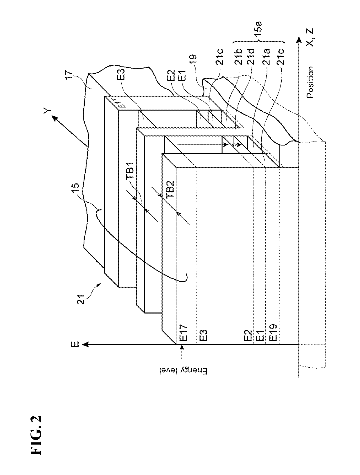
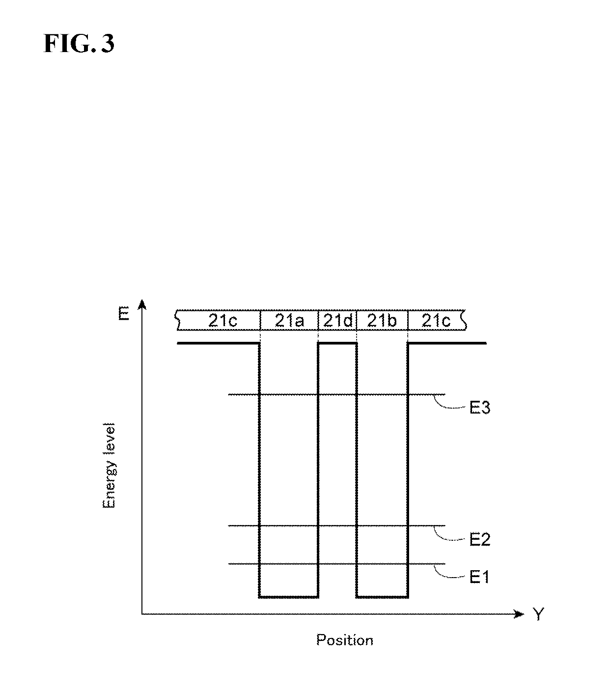
[0075]The quantum well structures will now be described with reference to FIG. 3. In the following description, electrons function as carriers. Similarly, holes may function as carriers. To increase the probability of transitions from the upper energy level E3 to the lower energy level E2, it is preferred to decrease the carrier density at the lower energy level E2. The decrease of the carrier density at the lower energy level E2 is realized by quickly transiting carriers from the lower energy level E2 to a relaxation energy level E1. Each quantum well structure 21 includes, for example, a plurality of (e.g., two) well layers (21a and 21b) and one or a plurality of barrier layers provided between these well layers. The barrier layer 21d has a thickness smaller than that of the barrier layer 21c. Thus, the wave functions of electrons in the well layers (21a and 21b) extend through the barrier layer 21d into the well layers (21b and 21a) and are coupled to each other. This structure i...
example 2
[0086]As shown in FIG. 4, at least a portion of a barrier layer in each quantum well structure may be doped with a dopant of the same polarity as the carriers. This doping improves the efficiency of injection into both well layers. For example, a 10 nm thick AlInAs barrier layer may include undoped thin region 21ca and 21cc adjacent to the well layers and a doped thin region 21cb therebetween. A doping concentration of about 1017 cm−3 or less is preferred to reduce optical loss due to free carrier absorption. This doped thin region improves the conductivity of the stacked semiconductor layer in the active region in the in-plane direction. As a result, carriers may be supplied to the well layers at positions apart from the emitter region in the in-plane direction.
example 3
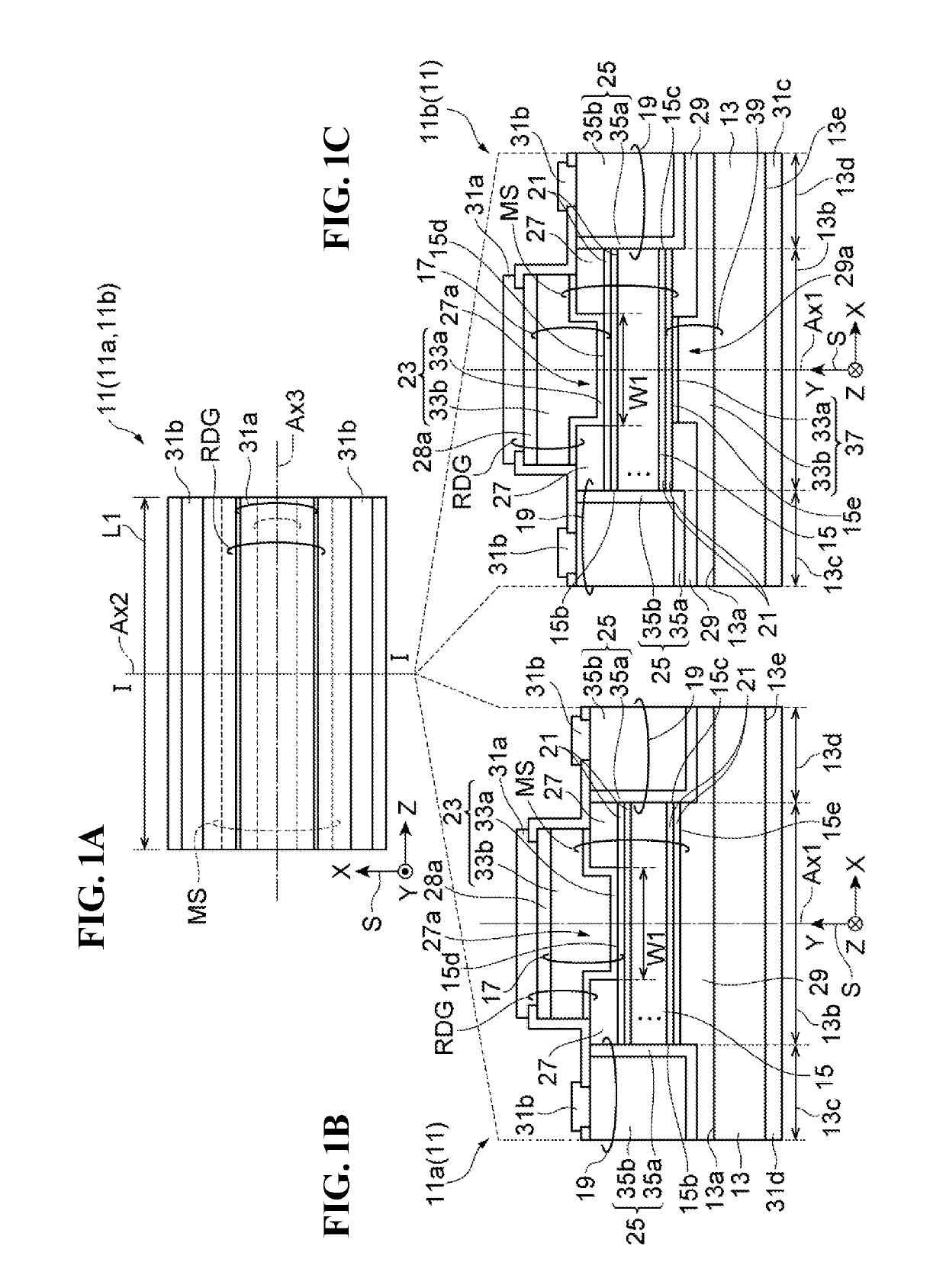
[0087]In the semiconductor laser 11 according to this embodiment, carriers are injected from the emitter region 17 into the quantum well structures 21 in the active region 15 in the direction of the first axis Ax1 and are thereby supplied to each quantum well structure 21. The carriers in the quantum well structures 21 are transported in a direction parallel to the in-plane direction of the quantum well layers. The electron distribution in the active region is estimated by simulation. To estimate carrier transport in the in-plane direction, the device models used for numerical experimentation are shown below.[0088]Resonator length L1: 500 μm[0089]Opening width W of emitter region: 10 μm[0090]One-side mesa width from center of opening in emitter region on active region in mesa structure to one upper edge of top surface of mesa: 10 μm[0091]One-side mesa width from center of opening in emitter region on active region in mesa structure to other upper edge of top surface of mesa: 10, 20,...
PUM
 Abstract
Description
Claims
Application Information