Semiconductor device, display panel, and electronic device

a technology of semiconductor devices and electronic devices, applied in the direction of instruments, portable computer details, electrical apparatus casings/cabinets/drawers, etc., can solve the problems of monotonic increase of output voltage, low response speed, and inability to obtain desired grayscale display, etc., to achieve increase in the number of switches, high resistance to voltage, and large circuit area

Active Publication Date: 2019-06-18
SEMICON ENERGY LAB CO LTD
View PDF6 Cites 2 Cited by
  • Summary
  • Abstract
  • Description
  • Claims
  • Application Information

AI Technical Summary

Benefits of technology

[0010]As described above, there are a variety of structures of semiconductor devices functioning as grayscale voltage generator circuits. The structures have merits and demerits, and an appropriate structure is selected in accordance with circumstances. For example, when a current DAC is employed as in Patent Document 2, a switch is composed of a transistor with high withstand voltage. The increase in the number of switches due to the increase in the number of bits of digital signals causes a larger circuit area. Moreover, the increase in the number of switches due to a larger number of digital signal bits causes the increase in parasitic capacitance of an output portion, resulting in lower response speed.
[0012]An object of one embodiment of the present invention is to provide a grayscale voltage generator circuit which is less likely to be influenced by an offset voltage. An object of one embodiment of the present invention is to provide a grayscale voltage generator circuit with a small area. An object of one embodiment of the present invention is to provide a novel grayscale voltage generator circuit. An object of one embodiment of the present invention is to provide a display panel with improved display quality. An object of one embodiment of the present invention is to provide a novel semiconductor device.
[0022]One embodiment of the present invention can provide a grayscale voltage generator circuit which is less likely to be influenced by an offset voltage. One embodiment of the present invention can provide a grayscale voltage generator circuit with a small area. One embodiment of the present invention can provide a novel grayscale voltage generator circuit. One embodiment of the present invention can provide a display panel with improved display quality. One embodiment of the present invention can provide a novel semiconductor device.

Problems solved by technology

Moreover, the increase in the number of switches due to a larger number of digital signal bits causes the increase in parasitic capacitance of an output portion, resulting in lower response speed.
If the output voltage which is influenced by the offset voltage exceeds a desired grayscale voltage, monotonic increase of the output voltage might be lost and desired grayscale display might not be obtained.

Method used


Image

  • Semiconductor device, display panel, and electronic device
  • Semiconductor device, display panel, and electronic device
  • Semiconductor device, display panel, and electronic device

Examples


embodiment 1

[0056]In this embodiment, an example of a semiconductor device functioning as a grayscale voltage generator circuit will be described.

10>

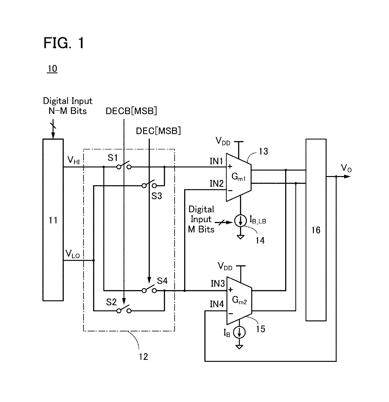
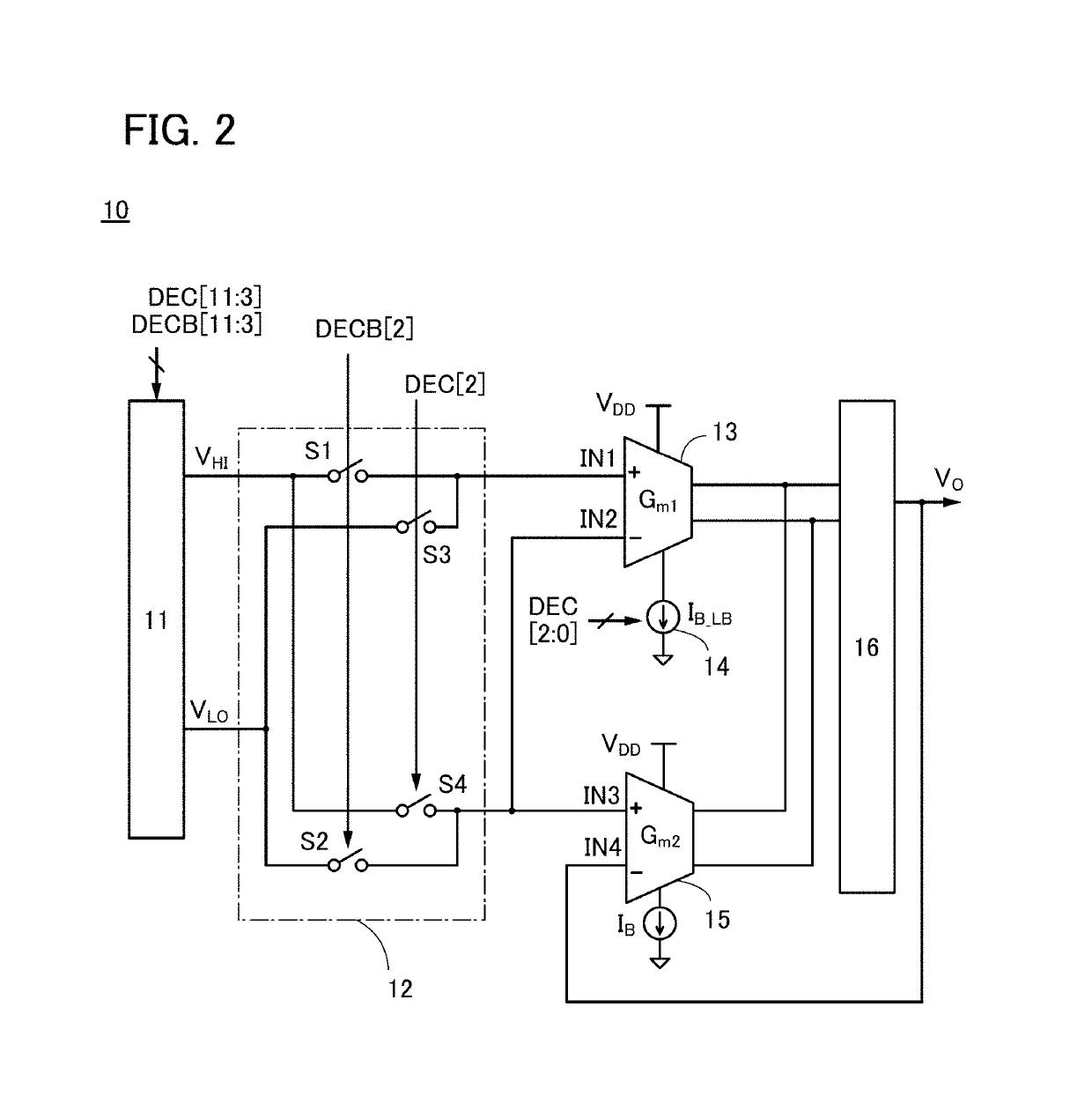
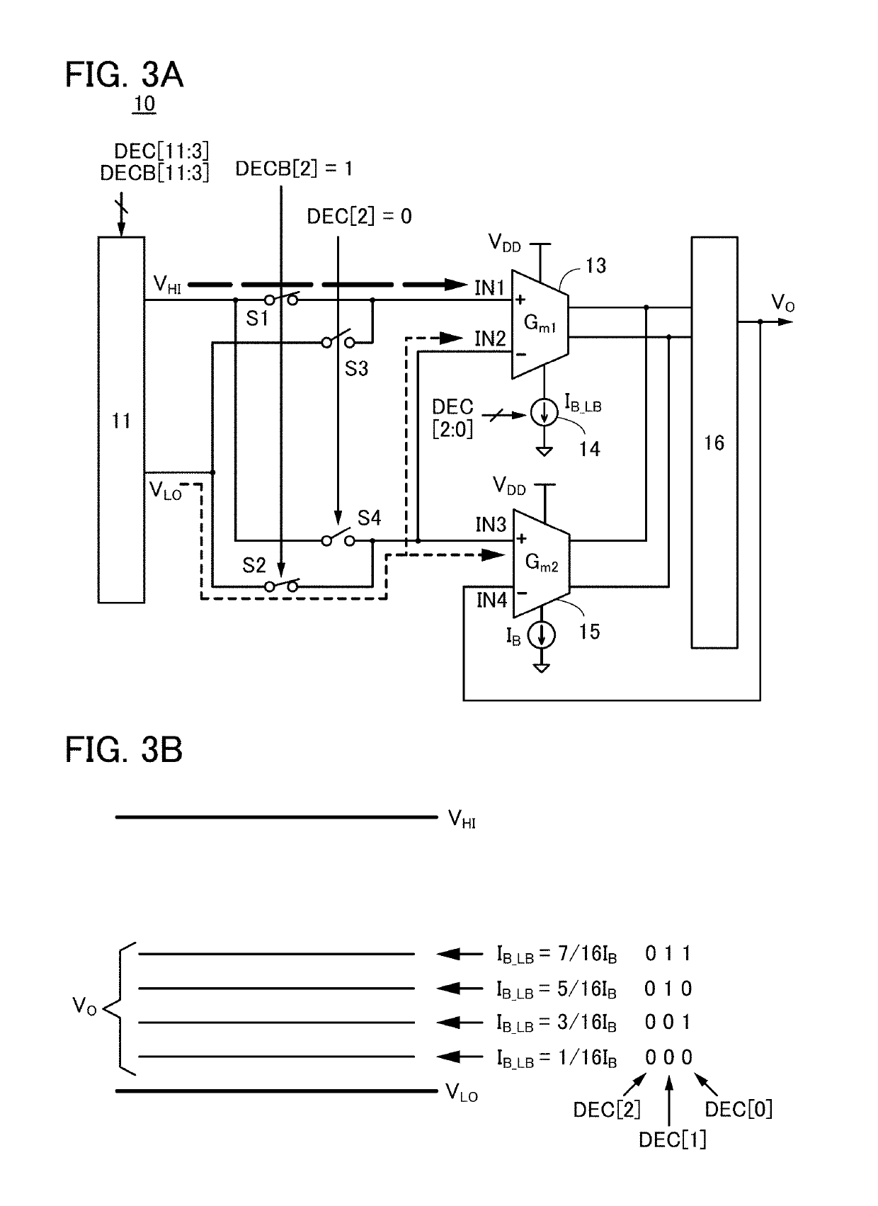
[0057]FIG. 1 is a circuit diagram illustrating an example of a circuit configuration for describing a semiconductor device 10. The semiconductor device 10 includes a digital-to-analog converter circuit (D / A converter circuit) 11, a selector circuit 12, an amplifier circuit 13, a current control circuit 14, an amplifier circuit 15, and an output buffer 16.

[0058]The amplifier circuit 13 is represented by a first Gm amplifier or Gm1 in some cases. The amplifier circuit 15 is represented by a second Gm amplifier or Gm2 in some cases.

[0059]The semiconductor device 10 has a function of converting an N-bit image signal (N is a natural number of 2 or more) into an analog signal represented by a voltage VO to output the analog signal.

[0060]The D / A converter circuit 11 is a circuit that converts an upper (N−M)-bit image signal (such a signal is hereinafter r...

embodiment 2

[0103]In this embodiment, a display panel including the semiconductor device 10 described in Embodiment 1 is described.

[0104]A display panel in a block diagram of FIG. 12 includes a signal line driver circuit 100, a scan line driver circuit 101, and a pixel portion 102. In the pixel portion 102, pixels 103 are arranged in a matrix. The pixel portion 102 may be referred to as a display portion.

[0105]The signal line driver circuit 100 has a function of outputting an image signal that has been converted into an analog signal to a plurality of signal lines SL.

[0106]A circuit included in the signal line driver circuit 100 may be an IC or may be formed using the same transistor as that in the pixel 103 in the pixel portion 102. Note that a plurality of signal line driver circuits 100 may be provided to control the signal lines SL separately.

[0107]The scan line driver circuit 101 has a function of outputting scan signals to scan lines GL. The scan line driver circuit 101 includes a shift r...

embodiment 3

[0146]In this embodiment, a more specific structure example of the display panel described in the above embodiments is described with reference to FIGS. 17A to 17C, FIGS. 18A to 18C, FIGS. 19A and 19B, FIGS. 20A and 20B, and FIGS. 21A and 21B. In this embodiment, a display panel including a liquid crystal element and a display panel including a light-emitting element are described as examples of the display panel.

[0147]FIGS. 17A to 17C are top views each illustrating a structure example of a display panel.

[0148]In FIG. 17A, a sealant 4005 is provided so as to surround the pixel portion 102 provided over a first substrate 4001, and the pixel portion 102 is sealed by the sealant 4005 and a second substrate 4006. In FIG. 17A, the signal line driver circuit 100 and the scan line driver circuit 101 are each formed using a single crystal semiconductor or a polycrystalline semiconductor over a substrate separately prepared and mounted in a region different from the region surrounded by the...


PUM


Abstract

A grayscale voltage generator circuit that is less likely to be influenced by the offset voltage is provided. The grayscale voltage generator circuit is a semiconductor device that includes a D / A converter circuit, a first Gm amplifier, a second Gm amplifier, a current control circuit, an output buffer, and a selector circuit. The D / A converter circuit generates a first voltage and a second voltage from an upper bit of a digital signal. The current control circuit generates a first current from a lower bit of the digital signal and functions as a current source of the first Gm amplifier. The output buffer generates a third voltage from currents output from the first Gm amplifier and the second Gm amplifier. The third voltage is input to the second Gm amplifier. The selector circuit selects voltages that are to be input to the first Gm amplifier and the second Gm amplifier.

Description

BACKGROUND OF THE INVENTION[0001]1. Field of the Invention[0002]One embodiment of the present invention relates to a semiconductor device, a display panel, and an electronic device.[0003]Note that one embodiment of the present invention is not limited to the above technical field. The technical field of the invention disclosed in this specification and the like relates to an object, a method, or a manufacturing method. Furthermore, one embodiment of the present invention relates to a process, a machine, manufacture, or a composition of matter. Specifically, examples of the technical field of one embodiment of the present invention disclosed in this specification include a semiconductor device, a display device, a light-emitting device, a power storage device, a memory device, a method for driving any of them, and a method for manufacturing any of them.[0004]In this specification and the like, a semiconductor device generally means a device that can function by utilizing semiconducto...

Claims


Application Information

Patent Timeline
Patent Type & Authority Patents(United States)
IPC IPC(8): G09G3/28H05K5/00G09G3/3266H01L27/32G06F3/041G09G3/36G06F1/16H01L27/12G09G3/20G09G3/3291G09G3/3225G09G3/3233
CPCG09G3/2007G06F1/163G06F1/1626G06F3/041G09G3/3225G09G3/3266G09G3/3291G09G3/3688H01L27/1225H01L27/3276H05K5/0017H05K5/0086G09G3/2003G09G3/3233G09G3/3696G09G2300/0828G09G2300/0842G09G2310/027G09G2310/0289G09G2310/0291G09G2310/08G09G2320/0233G09G2330/028G06F3/0412H10K59/131
Inventor TAKAHASHI, KEI
Owner SEMICON ENERGY LAB CO LTD
Why Eureka
Try Eureka