Unlock instant, AI-driven research and patent intelligence for your innovation.

Power amplification circuit

a power amplifier and circuit technology, applied in the direction of negative feedback circuit arrangement, single-ended push-pull amplifier, amplifier with semiconductor devices/discharge tubes, etc., can solve the problem of shortening the frequency band that can be allocated, low high-frequency performance, and cmos-produced wireless ics. the effect of reducing the power consumption and reducing the cost of production

Inactive Publication Date: 2019-06-18
PANASONIC CORP
View PDF2 Cites 0 Cited by
  • Summary
  • Abstract
  • Description
  • Claims
  • Application Information

AI Technical Summary

Benefits of technology

The patent text describes a power amplification circuit that can prevent an increase in power consumption and operate efficiently at a high gain. This means that the circuit can maintain stable operation while consuming less power.

Problems solved by technology

With increase in utilization of wireless technology, typified by communications and radars, shortage of frequency bands that can be allocated has been occurring in recent years.
The wireless ICs manufactured by the CMOS process, however, are low in high-frequency performance and for example, have difficulty in obtaining power gain at high frequencies, compared to those manufactured by another process.
In the circuit disclosed in “A 60 GHz CMOS Power Amplifier Using Capacitive Cross-Coupling Neutralization with 16% PAE” in EuMC 2011, however, power consumption increases because of its configuration where a differential signal is input and output.

Method used


Image

  • Power amplification circuit
  • Power amplification circuit
  • Power amplification circuit

Examples


first embodiment

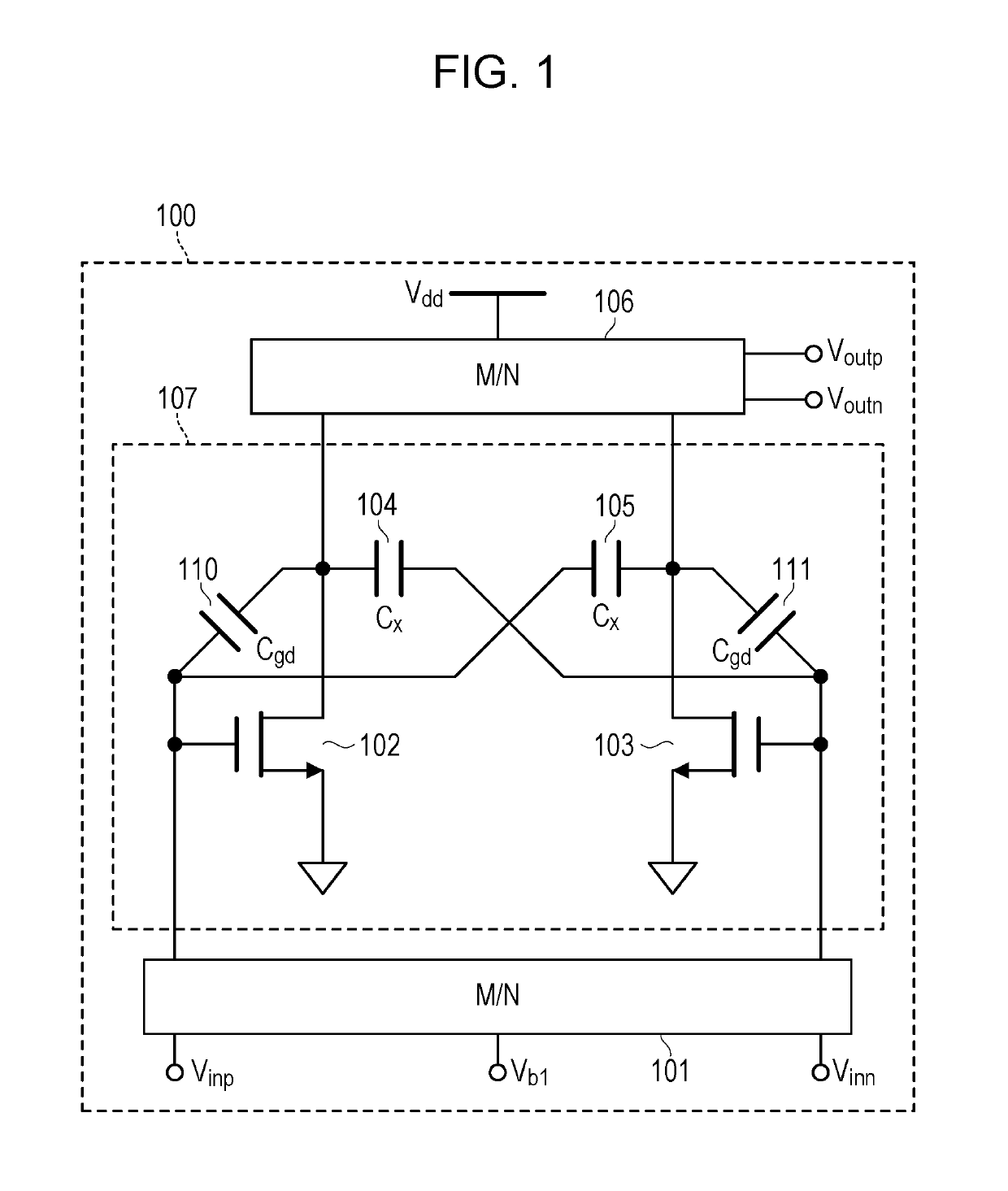
[0042]FIG. 2 illustrates a configuration example of a power amplification circuit 200 according to a first embodiment of the present disclosure.

[0043]The power amplification circuit 200 illustrated in FIG. 2 includes a transistor 201, a capacitor 202, a transformer 203, an input circuit 204, and an output circuit 205.

[0044]The input circuit 204 performs impedance conversion so as to adjust matching between a core unit 208, which includes the transistor 201, the capacitor 202, and the transformer 203, and a terminal of a circuit (not illustrated) that generates an input signal Vin.

[0045]The input signal Vin is input to the gate terminal of the transistor 201 through the input circuit 204. The source terminal of the transistor 201 is coupled to a ground (GND) and supplied with a voltage of 0 V. The source terminal of the transistor 201 may be coupled to a DC power supply that supplies a voltage except 0 V. The drain terminal of the transistor 201 is coupled to the output circuit 205.

[...

second embodiment

[0079]FIG. 5 illustrates a configuration example of a power amplification circuit 300 according to a second embodiment. In FIG. 5, identical reference denotations are given to constituent parts similar to those in FIG. 2 and descriptions thereof are omitted.

[0080]In a core unit 308 of the power amplification circuit 300, the transformer 203 of the power amplification circuit 200 in FIG. 2 is replaced with a transformer 303.

[0081]The transformer 303 includes an inductor 206, an inductor 207, and a resistor 301.

[0082]The resistor 301 is coupled in series to the inductor 206. The resistor 301 has a resistance value RFB. The resistor 301 may be a metal resistor or be a wiring resistor that uses part of a wiring pattern. The resistance value RFB is for example, approximately a few ohms to a few tens of ohms.

[0083]Although FIG. 5 illustrates an example where the resistor 301 is coupled between a terminal T2 of a capacitor 202 and a terminal T3 of the inductor 206, the resistor 301 may be ...

third embodiment

[0089]FIG. 7 illustrates a configuration example of a power amplification circuit 400 according to a third embodiment. In FIG. 7, identical reference denotations are given to constituent parts similar to those in FIG. 2 and descriptions thereof are omitted.

[0090]Compared to the power amplification circuit 200 in FIG. 2, a transistor 401 is added to a core unit 408 in the power amplification circuit 400.

[0091]The transistor 401 is a cascode transistor that undergoes concatenation with (is cascode-coupled to) a transistor 201. The gate terminal of the transistor 401 is coupled to a DC power supply and supplied with a voltage of Vb2 V. Although being set independently of Vdd, Vb2 is for example, identical in value to Vdd, such as 0.9 V to 1.8 V. Further, Vb2 is set to a value independent of Vb1. For example, Vb2 is larger in value than Vb1. The source terminal of the transistor 401 is coupled to the drain terminal of the transistor 201.

[0092]The drain terminal of the transistor 401 is ...


PUM


Abstract

A power amplification circuit includes a first transistor, which includes a source coupled to a first power supply and receives an input signal at a gate of the first transistor, a capacitor, which includes a first terminal and a second terminal, the first terminal being coupled to a drain of the first transistor, and a transformer, which is coupled between the second terminal and the gate of the first transistor, transforms a first signal input from the second terminal, and outputs a second signal having a phase different from a phase of the first signal to the gate of the first transistor. The first transistor outputs an output signal from the drain of the first transistor.

Description

BACKGROUND1. Technical Field[0001]The present disclosure relates to power amplification circuits.2. Description of the Related Art[0002]With increase in utilization of wireless technology, typified by communications and radars, shortage of frequency bands that can be allocated has been occurring in recent years. To address such frequency shortage, for example, high-frequency bands, which generally include a millimeter wave band and a terahertz band, are utilized. For example, a 60 GHz band is used in communication through a millimeter wave band and a 79 GHz band is used by a millimeter wave radar. Since it is expected that wireless integrated circuits (ICs) that operate using a millimeter wave band and a terahertz band will be more widespread, manufacturing the wireless ICs at low cost is under review.[0003]A typical wireless IC is made of a semiconductor and manufactured by a complementary metal-oxide-semiconductor (CMOS) process. The CMOS process enables manufacture of wireless IC...

Claims


Application Information

Patent Timeline
Patent Type & Authority Patents(United States)
IPC IPC(8): H03F3/45H03F1/34H03F3/30H03F1/56H03F3/195H03F1/02
CPCH03F1/56H03F3/195H03F3/3098H03F3/45179H03F3/45264H03F1/0216H03F1/347H03F2200/222H03F2200/387H03F2203/45318H03F2203/45332H03F2203/45394H03F1/0211H03F3/211H03F2203/45034
Inventor ABE, TAKAYUKI
Owner PANASONIC CORP