
Integrating a gate-all-around (GAA) field-effect transistor(s) (FET(S)) and a finFET(s) on a common substrate of a semiconductor die

a field-effect transistor and gate-all-around technology, applied in the field of gate-all-around transistors, can solve the problems of increasing current leakage, degrading performance, and complex functionality of electronic devices, and achieve the effects of reducing resistance and capacitance, reducing threshold voltage, and reducing supply voltag

Active Publication Date: 2019-06-25
QUALCOMM INC
View PDF15 Cites 27 Cited by
  • Summary
  • Abstract
  • Description
  • Claims
  • Application Information

AI Technical Summary

Benefits of technology

This patent describes integrating two types of field-effect transistors (FETs) on a common substrate of a semiconductor die. This allows for the use of each type of FET for different circuit applications, optimizing their strengths while minimizing their weaknesses. For example, some circuits may require a reduced threshold voltage to lower power consumption, while other circuits may require faster performance. By integrating these FETs on a common substrate, a designer has more freedom to independently control their channel width and drive strength. This results in improved performance and lower power consumption for the integrated circuit.

Problems solved by technology

As electronic devices become more complex in functionality, so does the need to include a greater number of transistors in such devices.
However, as channel length in planar transistors is reduced such that the channel length is of the same order of magnitude as the depletion layers widths, short channel effects (SCEs) can occur that degrade performance.
More specifically, SCEs in planar transistors can cause increased current leakage, reduced threshold voltage, and / or threshold voltage roll-off (i.e., reduced threshold voltage at shorter gate lengths).
There is continued pressure to improve the processing capabilities of ICs, which results in pressure to increase a number of transistors present on a given IC.
However, disadvantages of GAA FETs are increased resistance resulting in increased current-resistance (IR) drop and increased capacitance due to coupling between source / drain and gate.
GAA FETs also suffer from an area penalty over FinFETs when more than one active semiconductor fin is employed for drive strength requirements.
Thus, the performance advantages of GAA FETs versus FinFETs may diminish for high-performance blocks such as CPU cells, memory cells and input / output (I / O) cells.

Method used


Image

  • Integrating a gate-all-around (GAA) field-effect transistor(s) (FET(S)) and a finFET(s) on a common substrate of a semiconductor die
  • Integrating a gate-all-around (GAA) field-effect transistor(s) (FET(S)) and a finFET(s) on a common substrate of a semiconductor die
  • Integrating a gate-all-around (GAA) field-effect transistor(s) (FET(S)) and a finFET(s) on a common substrate of a semiconductor die

Examples


Embodiment Construction

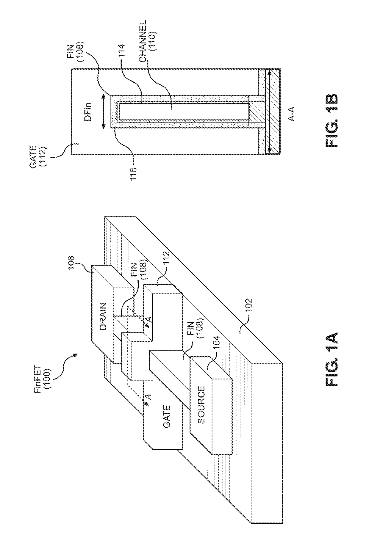
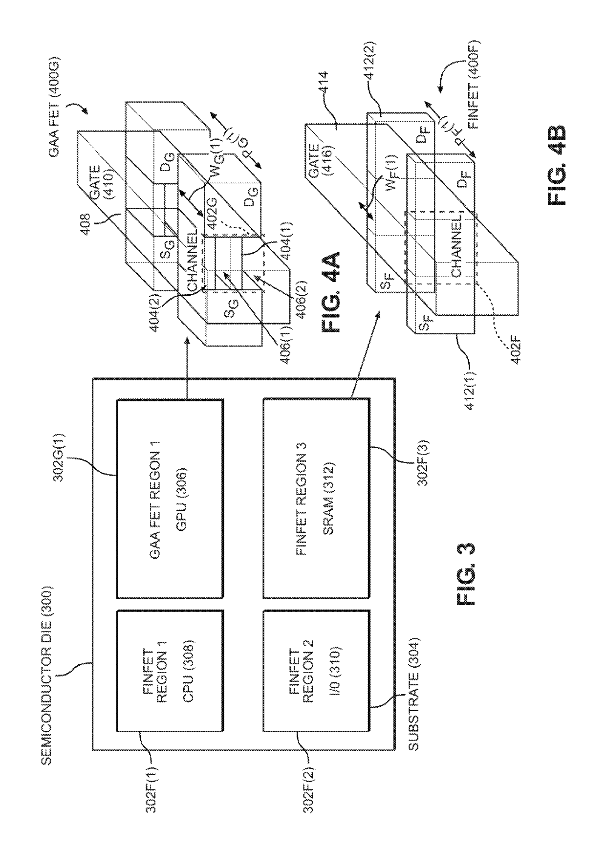
[0044]With reference now to the drawing figures, several exemplary aspects of the present disclosure are described. The word “exemplary” is used herein to mean “serving as an example, instance, or illustration.” Any aspect described herein as “exemplary” is not necessarily to be construed as preferred or advantageous over other aspects.

[0045]Aspects disclosed herein include integrating a gate-all-around (GAA) field-effect transistor(s) (FET(s)) and a FinFET(s) on a common substrate of a semiconductor die. Related methods are also disclosed. GAA FETs and FinFETs can be employed to form integrated circuits (ICs). In exemplary aspects disclosed herein, GAA FETs and FinFETs are integrated on a common substrate to optimize advantages of each type of FET for different circuit applications in a semiconductor die. Thus, FinFETs may be formed with the common substrate in the semiconductor die for forming circuits where reduced resistance and capacitance are important for performance, whereas...


PUM


Abstract

Integrating a gate-all-around (GAA) field-effect transistor(s) and a FinFET(s) on a common substrate of a semiconductor die is disclosed. GAA FETs and FinFETs can form integrated circuits (ICs). GAA FETs and FinFETs are integrated on a common substrate to optimize advantages of each type of FET. For example, FinFETs may be formed in the common substrate in the semiconductor die for forming circuits where reduced resistance and capacitance are important for performance, whereas GAA FETs may be formed in the common substrate in the semiconductor die for forming circuits with decreased threshold voltage to allow voltage scaling to lower supply voltages to reduce power consumption and also to reduce silicon area as a result of vertically stacked devices. This supports a designer having the freedom to separate control the channel width of the GAA FETs and FinFETs, which may be important for controlling drive strength and / or area for different circuits.

Description

BACKGROUNDI. Field of the Disclosure[0001]The technology of the disclosure relates generally to semiconductor devices forming integrated circuits (ICs), and more specifically, to gate around transistors, such as Fin Field-Effect Transistors (FETs) (FinFETs) and gate-all-around (GAA) transistors (e.g., nanowire, nanoslab, nanosheet transistors).II. Background[0002]Transistors are essential components in modern electronic devices. Large numbers of transistors are employed in integrated circuits (ICs) in many modern electronic devices. For example, components such as central processing units (CPUs), graphics processing units (GPUs), and memory systems each employ a large quantity of transistors for logic circuits and memory devices.[0003]As electronic devices become more complex in functionality, so does the need to include a greater number of transistors in such devices. But as electronic devices are required to be provided in increasingly smaller packages, such as in mobile devices f...

Claims


Application Information

Patent Timeline
IPC IPC(8): H01L21/02H01L27/02H01L21/8234H01L29/423H01L27/088H01L21/762H01L21/306H01L29/66H01L27/11H01L29/06
CPCH01L27/0886H01L29/0673H01L29/0649H01L27/0207H01L21/823412H01L21/823431H01L21/823481H01L21/76224H01L21/30625H01L29/66545H01L21/823437H01L21/02532H01L21/02381H01L29/6656H01L21/823418H01L29/42392H01L21/823475H01L27/1104H01L21/823456H01L29/775H01L29/66439H01L29/78696H01L27/1211B82Y10/00H10B10/12
Inventor BADAROGLU, MUSTAFARIM, KERN
Owner QUALCOMM INC
Learn More