Method and apparatus for alignment of a line-of-sight communications link

a communication link and line-of-sight technology, applied in the direction of line-of-sight transmission, electrical equipment, close-range type systems, etc., can solve the problems of inability to detect signals, no signal detection, and difficulty in achieving accurate alignment, so as to avoid interference, the effect of reducing the accuracy of the alignmen

Active Publication Date: 2019-08-06
OPTIPULSE INC
View PDF5 Cites 7 Cited by
  • Summary
  • Abstract
  • Description
  • Claims
  • Application Information

AI Technical Summary

Problems solved by technology

Failure to properly align the transmitter and receiver can lead to a noisy signal detected by the receiver or even no detection of the signal at the receiver if the misalignment is too great.
Achieving accurate alignment can be a challenging task, particularly when there is a long distance between transmitter and receiver.
Since such transmitters and receivers are often located on high towers or in other hard-to-reach places, manual alignment is not only slow and inefficient but can also be dangerous for the technicians.

Method used


Image

  • Method and apparatus for alignment of a line-of-sight communications link
  • Method and apparatus for alignment of a line-of-sight communications link
  • Method and apparatus for alignment of a line-of-sight communications link

Examples


embodiment 1

for US Pat App Pub 2017 / 0033535—Top-Emitting Implant

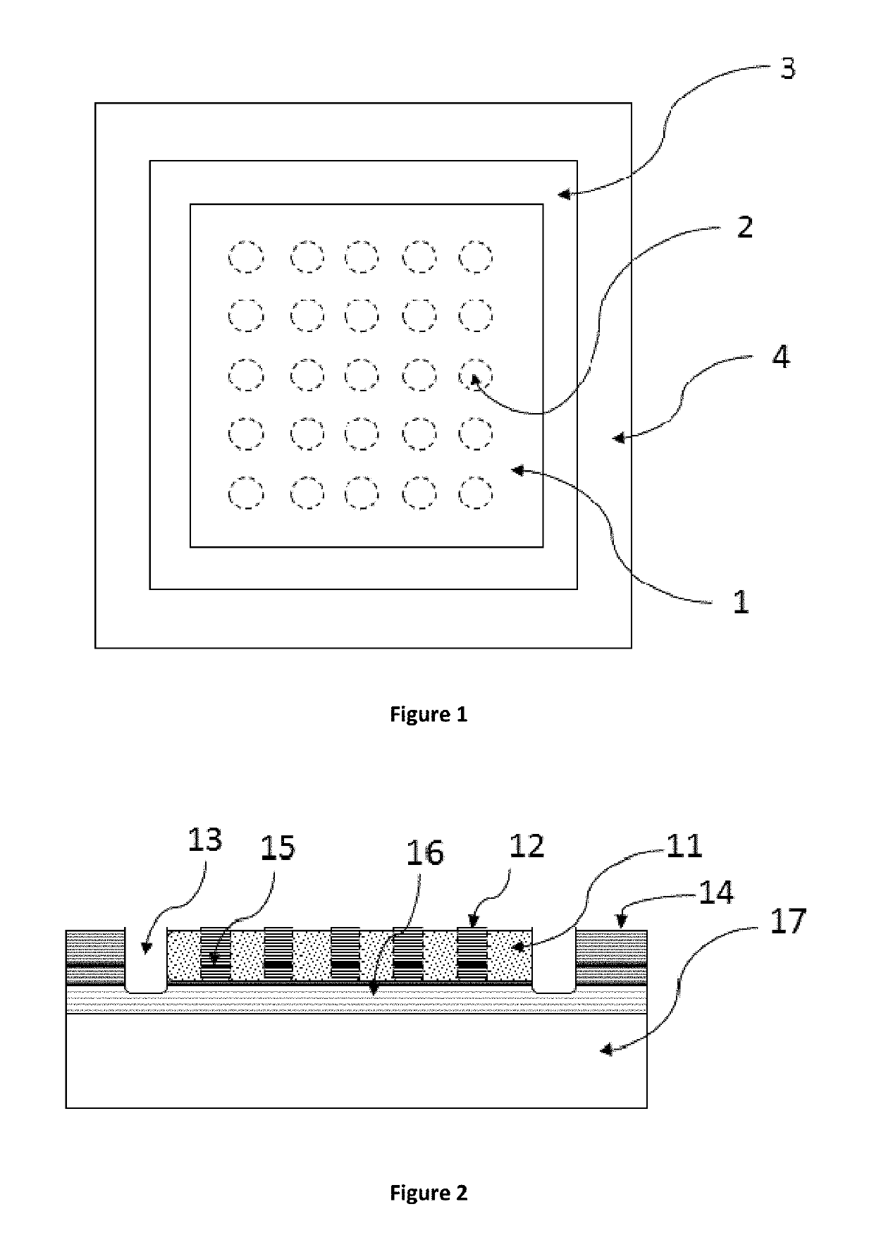
[0076]FIG. 1 shows an example of a first embodiment of the invention. In this example, a single solid structure is isolated from a surrounding ground with an etch, and where the single solid structure has within it ion implants. The ion implants create areas of the semiconductor material that are non-conductive, and these areas of non-conductivity force current flow through the lasing areas 2. Thus, the ion implants form a laser grid of multiple lasing areas 2 where current is confined to isolated regions in the structure where conductivity exists as compared to the nonconductive ion-implanted areas. The conductive and nonconductive areas form a grid of light which has a single metal contact on the single solid structure for the active positive (P) contact and a single negative (N) contact on the surrounding ground structure which is shorted to the N contact area at the bottom of the trench isolating the two areas or to negative me...

embodiment 2

for US Pat App Pub 2017 / 0033535—Bottom-Emitting Implant

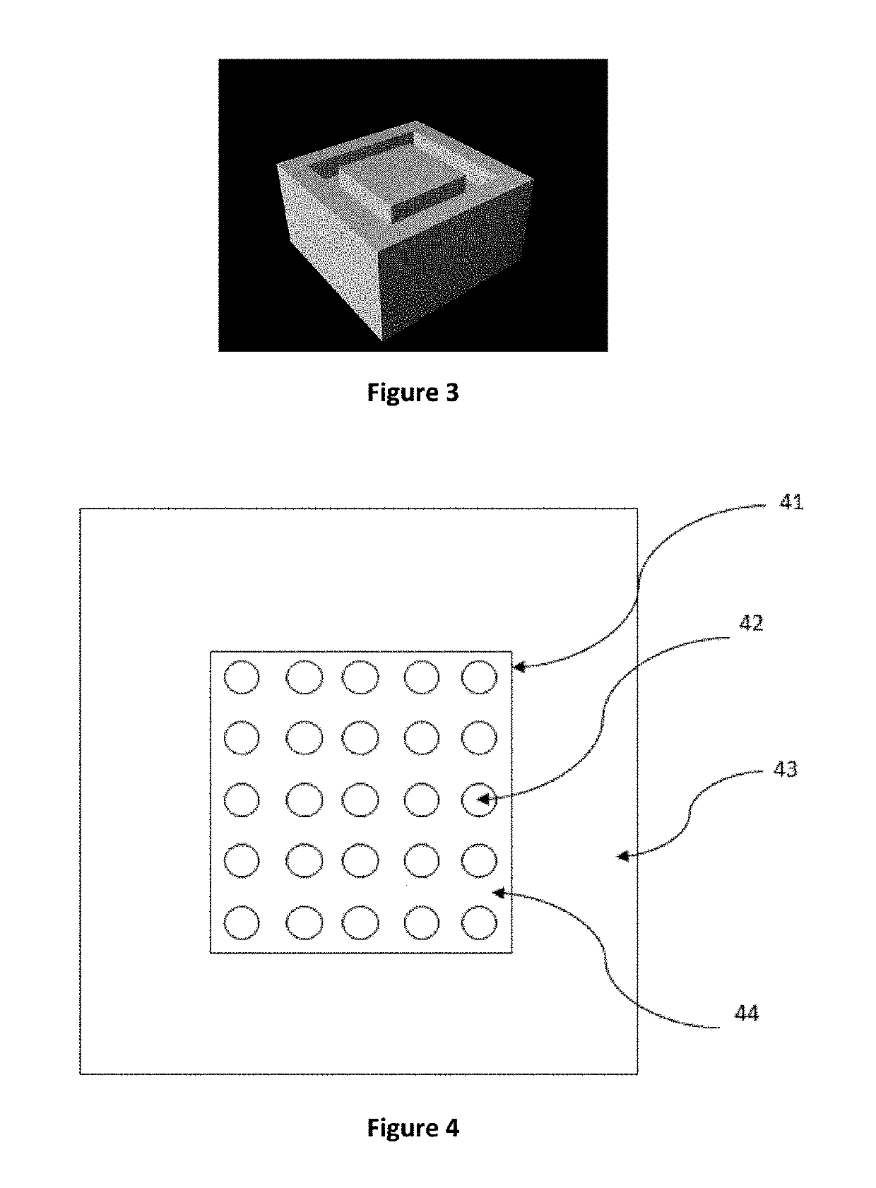
[0117]FIG. 6 illustrates a cutaway view of an example of a second embodiment, where the second embodiment is a bottom-emitting device with implanted regions for current confinement. The GSG electrical waveguide can be seen solder bonded to the frame-ground structure and the active single laser mesa structure. FIG. 6 shows:[0118]601 Electrical Waveguide Substrate[0119]602 Ground Contact and Signal Contact in that order of GSG Electrical Waveguide[0120]603 Solder-Bonding GSG Waveguide to Laser Chip[0121]604 Plating Metal electrically connecting Signal pad of Electrical Waveguide to Lasers P contact[0122]605 P contact Metal[0123]606 Implanted Region that has been rendered non conductive[0124]607 P mirror[0125]608 Active region (quantum wells)[0126]609 N Mirror[0127]610 Conducting Layers in N Mirror where Implant has not reached[0128]611 Laser Beams Propagating through Laser Substrate[0129]612 Plating Metal shorted to N contact regi...

embodiments 1 and 2

Process for Embodiments 1 and 2 of US Pat App Pub 2017 / 0033535

[0133]An example embodiment of the process steps to create the single structure for embodiments 1 and 2 with implant current confinement can be as follows.[0134]Step 1. Use photolithography to mask areas which will not have P Metal deposited.[0135]Step 2. Deposit P Metal (typically TiPtAu ˜2000 A)[0136]Step 3. Photolithography lift off and wafer cleaning. O2 descum or ash all organics off wafer.[0137]Step 4. Dielectric deposit (typically SiNx ˜[0138]Step 5. Photolithographic masking using either photoresist or metal deposited in areas to protect the epi material from being damaged from the implant which makes the unprotected regions non-conductive through ion bombardment. This step can be performed later in the process but may be more difficult due to more varied topology.[0139]Step 6. Implant—Those skilled in the art of calculating the implant doses will determine the dose and species of implant needed to disrupt the mat...


PUM


Abstract

Techniques are disclosed for aligning a first optical scope with a second optical scope to achieve a line-of-sight communication link between the two optical scopes. In an example embodiment, each scope can include an optical transceiver and camera. The optical transceiver in the first optical scope can include a light array that is used to emit a bright pulse of light as a flash. The camera in the second optical scope captures this flash in a camera image. The camera image can then be processed to spatially localize the flash relative to a central region of a photodetector array in the optical transceiver of the second optical scope. A control system can then drive a positioning system for the second optical scope to adjust the second optical scope's positioning so that the second optical scope photodetector array's central region aligns with the spatially localized flash.

Description

CROSS REFERENCE AND PRIORITY CLAIM TO RELATED PATENT APPLICATION[0001]This patent application claims priority to U.S. provisional patent application Ser. No. 62 / 554,735, filed Sep. 6, 2017, entitled “Method and Apparatus for Alignment of Line-Of-Sight Communications Link”, the entire disclosure of which is incorporated herein by reference.INTRODUCTION[0002]The use of free space optical communications (FSOC) for wireless data transfer via light beams relies on a line-of-sight communication link between transmitter and receiver, and such a line-of-sight communication link requires accurate alignment between transmitter and receiver. Failure to properly align the transmitter and receiver can lead to a noisy signal detected by the receiver or even no detection of the signal at the receiver if the misalignment is too great. Achieving accurate alignment can be a challenging task, particularly when there is a long distance between transmitter and receiver.[0003]For example, optical transmi...

Claims


Application Information

Patent Timeline
Patent Type & Authority Patents(United States)
IPC IPC(8): H04B10/112H04B10/073H04B10/50
CPCH04B10/112H04B10/0731H04B10/503H04B10/1123H04B10/116
Inventor JOSEPH, JOHN RICHARD
Owner OPTIPULSE INC
Why Eureka
Try Eureka