Method and device for coating a product substrate

a technology for product substrates and coatings, applied in the direction of liquid spraying apparatus, electrical apparatus, lamination apparatus, etc., can solve the problems of large amount of coating, and large amount of coating, and achieve the effect of simple process steps, high throughput, and high application efficiency

Active Publication Date: 2019-08-27
EV GRP E THALLNER GMBH
View PDF53 Cites 0 Cited by
  • Summary
  • Abstract
  • Description
  • Claims
  • Application Information

AI Technical Summary

Benefits of technology

[0005]It is therefore an object of the present invention to provide a method and a device, with which the partial coating of product substrates can be achieved in an economical manner with as few as possible, preferably simple, process steps. The method and the device are to be as universally usable as possible and / or to have as high a throughput as possible.

Problems solved by technology

These direct coating methods in general always coat the entire surface.
In turn, this process therefore pertains to a complete coating of the surface, which is unacceptable for many applications.
In other applications, a brief contact with the coating material would be acceptable, but the removal of the same from the locations that are not to be coated represents a major problem.
Thus, for example, structures with a large height-to-width ratio can produce a very strong capillary effect, which makes the removal of the coating material from the structures impossible.
In addition, all types of masking techniques are very labor-intensive and costly, in particular since a relatively large number of process steps must be performed.
An increasing number of process steps increases not only the costs, but also the susceptibility to errors.
A technical problem lies in the fact that a μCP stamp must be adapted to transfer a material to the structures of the product wafers that are to be coated.
In addition, the problem lies in the fact that in a first process step, a μCP stamp must be immersed in the material that is to be transferred or must be impregnated with the material from its rear side.

Method used


Image

  • Method and device for coating a product substrate
  • Method and device for coating a product substrate
  • Method and device for coating a product substrate

Examples


Embodiment Construction

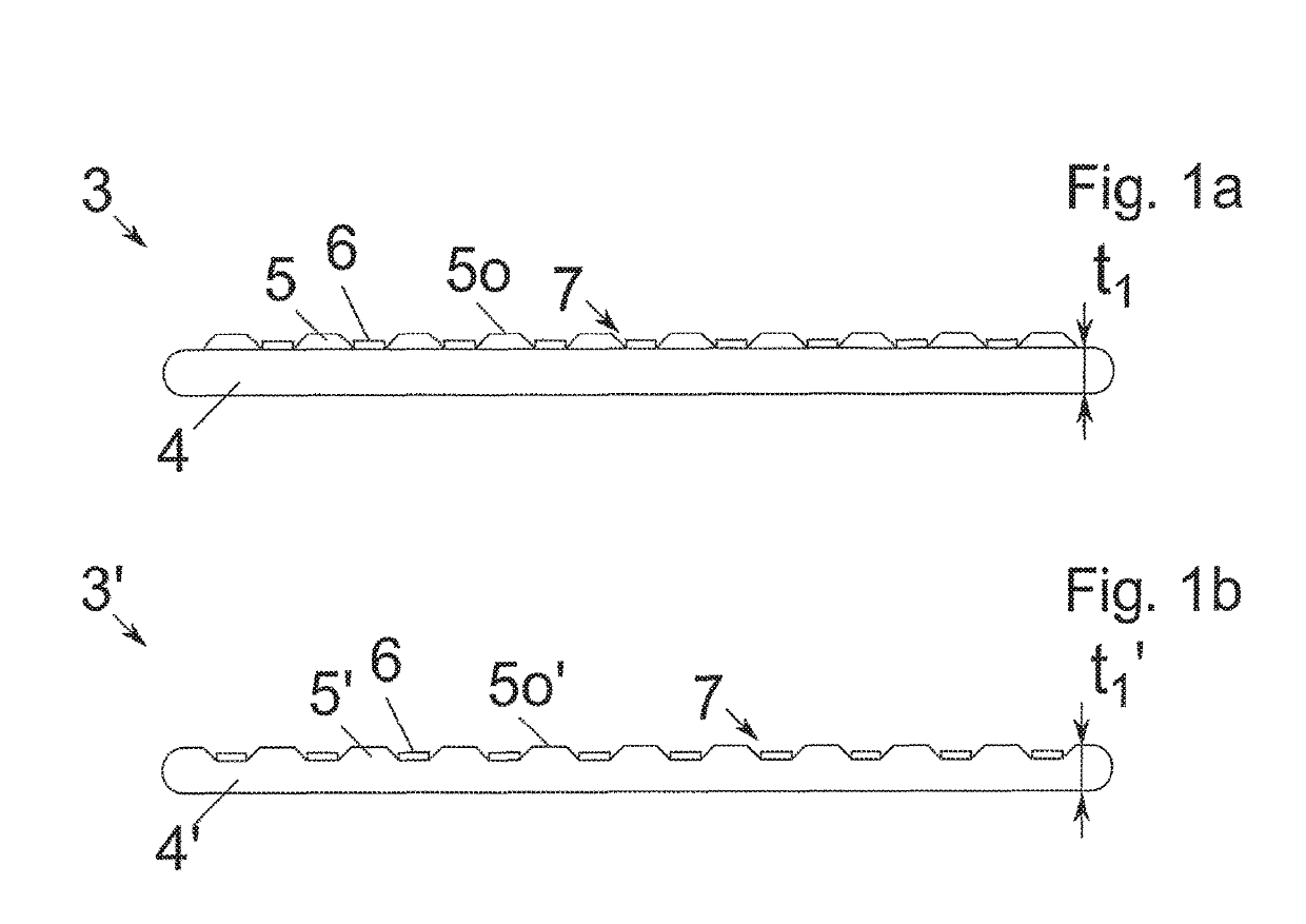
[0072]FIG. 1a shows a diagrammatic side view, not to scale, of a product substrate 3, comprising:[0073]A wafer 4, on which several projections 5 are formed,[0074]Functional units 6, which are to be encapsulated, are arranged between the projections 5.

[0075]The wafer 4 has a mean thickness t1. The entire thickness of the structured product substrate 3 is consequently greater than t1.

[0076]FIG. 1b shows a diagrammatic side view, not to scale, of a structured product substrate 3′, comprising:[0077]A wafer 4′, produced in particular by etching, with multiple projections 5, which are created by the etching of recesses 7,[0078]The functional units 6, which are to be encapsulated, are arranged between the projections 5, i.e., in the recesses 7.

[0079]The wafer 4′ has a mean thickness t1′. In this embodiment, the total thickness of the structured product substrate 3′ is in particular equal to the thickness t1′.

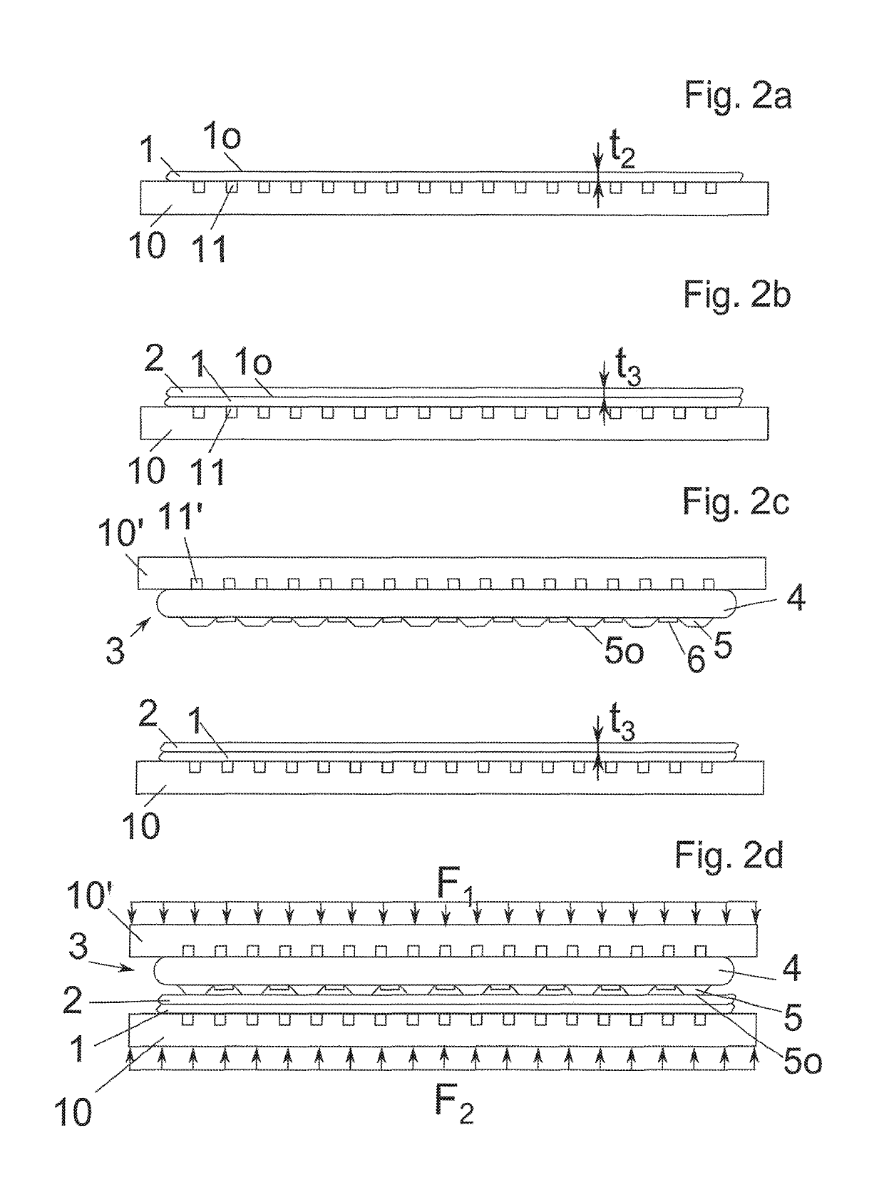
[0080]The first process step of the carrier substrate preparation according to the...


PUM

PropertyMeasurementUnit
lengthsaaaaaaaaaa
lengthsaaaaaaaaaa
lengthsaaaaaaaaaa

Abstract

A method and device for coating projecting surfaces of discrete projections of a product substrate that has functional units arranged at least partially in recesses. The method includes the steps of: bringing the projecting surfaces into contact with a coating material that is applied on a carrier substrate, and separating the carrier substrate from the projecting surfaces in such a way that the coating material remains partially on the product substrate. In addition, this invention relates to a corresponding device.

Description

FIELD OF INVENTION[0001]The invention relates to a method and a device for coating a product substrateBACKGROUND OF THE INVENTION[0002]In the semiconductor industry, there exist various methods for applying very thin layers, in particular layers with mean thicknesses in the micrometer range, or even in the nanometer range, on surfaces. Frequently, direct coating methods that deposit a material on a surface are used. These include, for example, chemical and physical gas phase deposition, dipping methods, etc. These direct coating methods in general always coat the entire surface.[0003]In the semiconductor industry, however, there are innumerable methods in which it is necessary to be sure not to coat the entire surface. In order to keep a coating from areas that are not to be coated, masking techniques, for example photolithography or imprint lithography, are still frequently used in the state of the art. In photo processes, however, the usual procedure is first to coat the entire su...

Claims


Application Information

Patent Timeline
Patent Type & Authority Patents(United States)
IPC IPC(8): H01L21/67B05B7/14B32B37/08B05B7/12
CPCH01L21/67132H01L21/67126H01L21/56B05B7/1272B05B7/1481B32B37/08
Inventor THANNER, CHRISTINE
Owner EV GRP E THALLNER GMBH
Why Eureka
Try Eureka