Generation of high-power spatially-restructurable spectrally-tunable beams in a multi-arm-cavity VECSEL-based laser system
a laser system and spatial restructuration technology, applied in the direction of lasers, lasers, semiconductor lasers, etc., can solve the problems of limiting the spectral tenability of the produced lg-laser beam, increasing the overall system cost, and limited power and/or operating wavelength rang
- Summary
- Abstract
- Description
- Claims
- Application Information
AI Technical Summary
Benefits of technology
Problems solved by technology
Method used
Image
Examples
embodiments
NON-LIMITING EXAMPLES OF EMBODIMENTS
Example 1
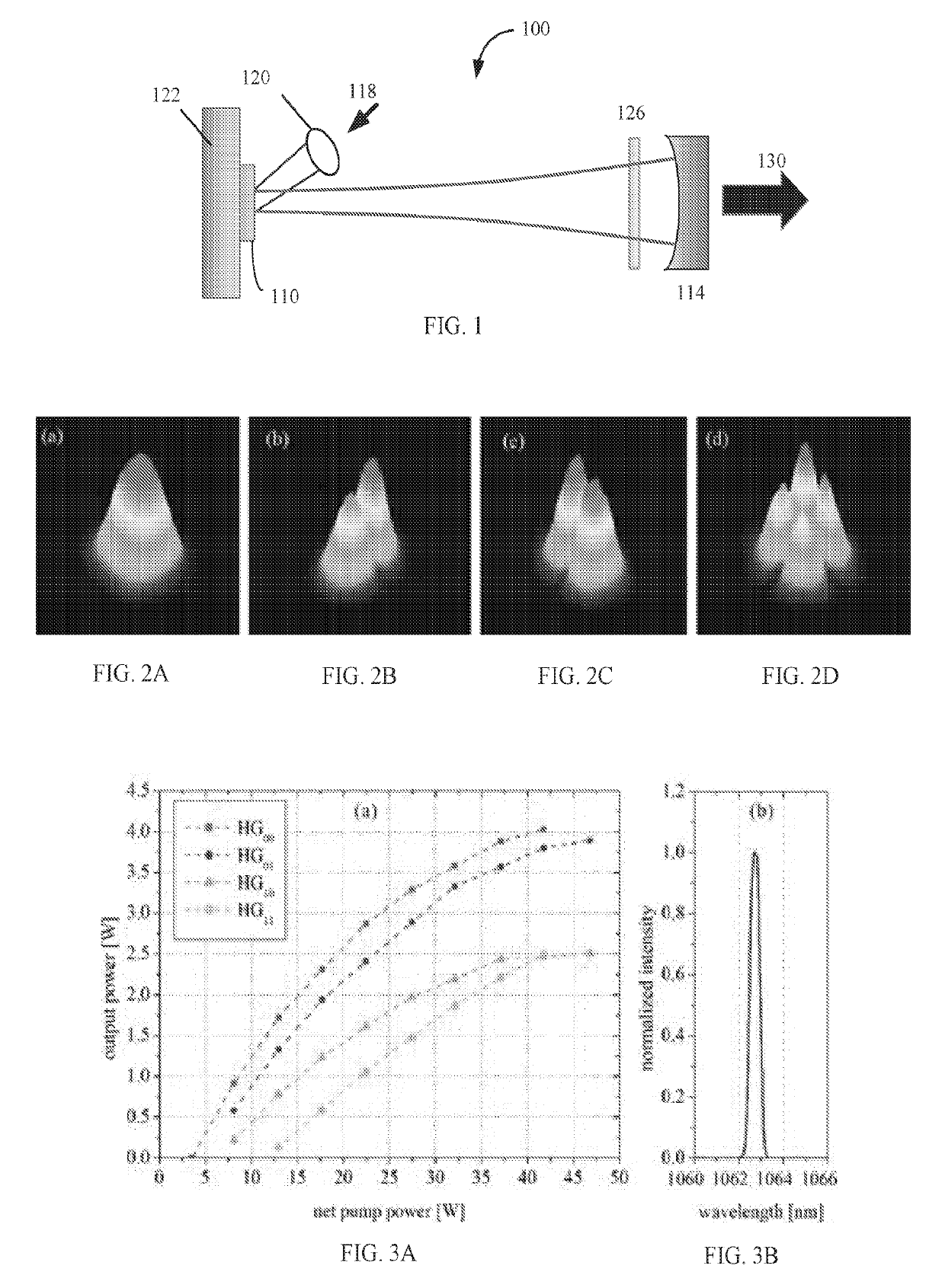
[0049]This implementation provides demonstrates that a linear-cavity VECSEL structure, containing an MCE intracavity, is enabled to control oscillation of the cavity field in a selected higher-order HG beam at the fundamental wavelength.
[0050]In the experiments reported here, MOCVD was used to grow a VECSEL heterostructure designed to emit at about 1070 nm. The active region included 12 compressively-strained 8-nm-thick InGaAs quantum wells (QWs) with GaAs-pump-absorbing barriers and a layer of GaAsP between each neighboring QWs for strain compensation. On top of the multi-quantum well (MQW) unit the 25 pairs of alternating AlGaAs / AlAs layers were grown to operate as a high reflectivity (˜99.9%) distributed Bragg reflector (DBR) at the emission wavelength. The specific thickness and composition of the heterostructure layers were judiciously chosen to achieve resonant periodic gain (RPG) such that each QW is positioned at the antinodes of ...
example 2
-Structured Beam Via SHG in a V-Cavity VCSEL
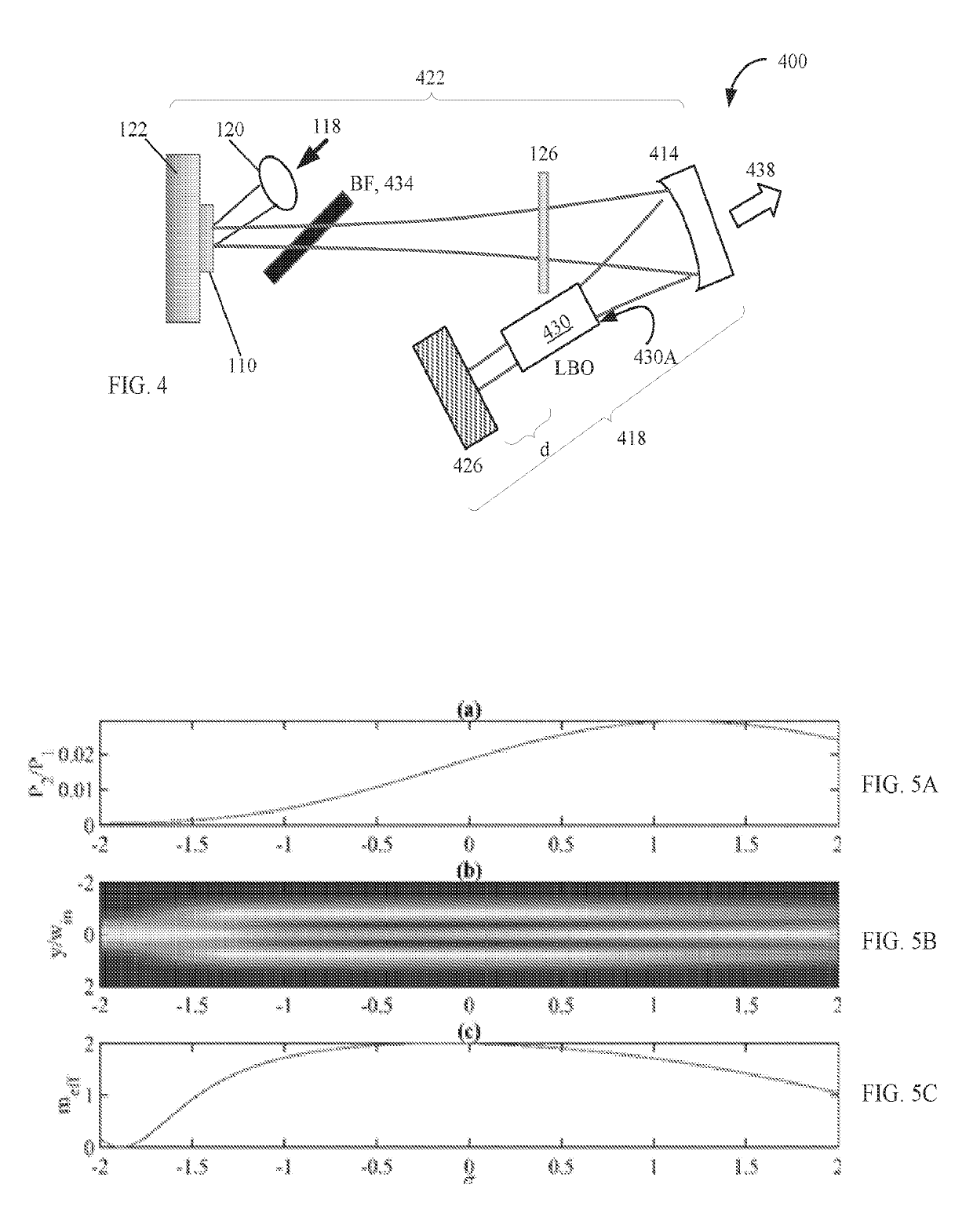
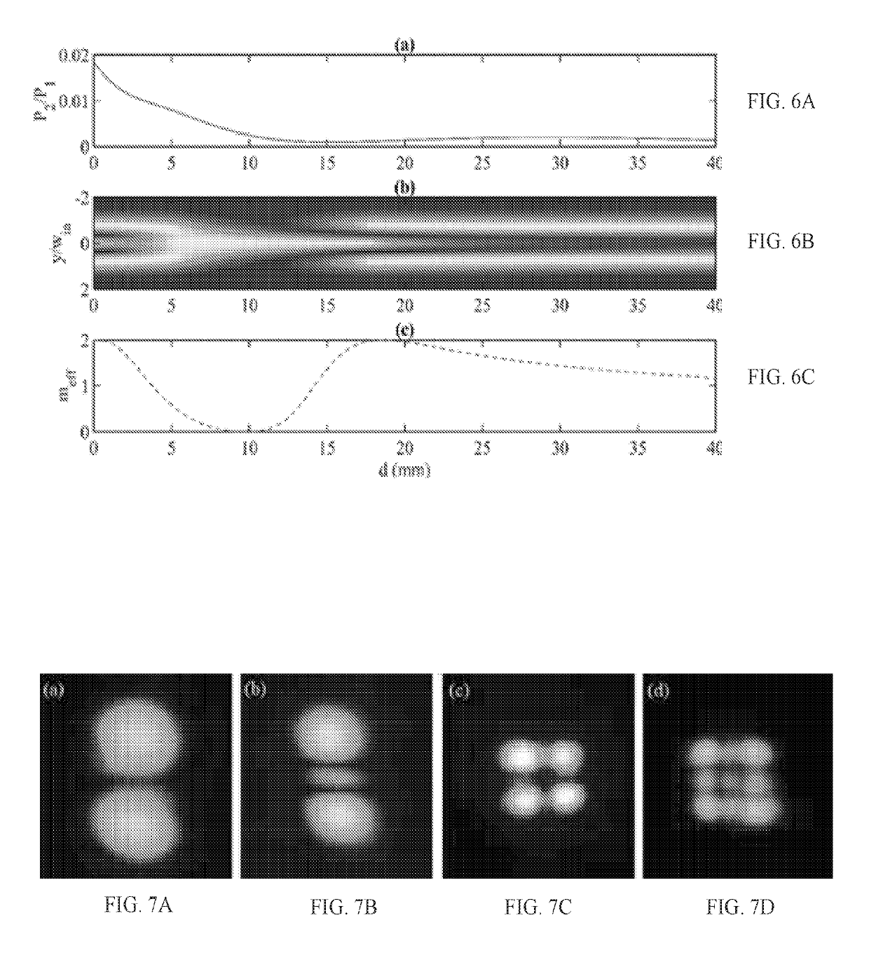
[0054]Here, as shown in FIG. 4, an embodiment 400 employed a common V-folded laser cavity configuration. This cavity type, compared to linear cavity of FIG. 1, is advantageous in the case of nonlinear conversion because it allows controlling the size of the transverse mode in both the gain medium and the nonlinear crystal. The spherical concave reflector 414 with a radius of curvature of 10 cm served as a folding mirror to form a folded portion of the cavity (“fold”) 418 folded with respect to the linear portion of the cavity 422, while the VECSEL chip 110 and the flat end reflector 426 defined and enclosed the overall resonant cavity. For SHG operation, an LBO crystal 430 (3×3×15 mm3; both facets AR coated for both 1075 nm and 537 nm), cut for type I angular phase-matching condition with angles θ=90° and ϕ=11°, was inserted into the shorter arm (fold 418) of the laser resonator a variable distance d away from the flat mirror 436. Both ref...
example 3
[0075]The separate VECSEL chips used in the experimental setup schematically depicted in FIG. 10 were fabricated from two different wafers with strain-compensated InGaAs / GaAs / GaAsP multi-quantum-well (MQW) heterostructures designed for emission at about 970 nm and at about 1070 nm. An MCVD process was utilized to grow the wafer in a “bottom-emitting” manner, such that the active region precedes a DBR on a GaAs substrate. To maximize the gain, in both chip structures the compositions and thicknesses of the gain regions were carefully chosen such that each QW were positioned at the antinode of the resonator standing wave—a design referred to herein as a resonant periodic gain. While both structures have active regions consisting of 12 compressively strained 8 nm thick InGaAs QWs with pump absorbing GaAs barriers and GaAsP layer between each QW for strain compensation purposes, the semiconductor compositions slightly varied between the wafers used for 970 nm and 1070 nm chips. Similarl...
PUM
 Abstract
Description
Claims
Application Information


