Supercharge Your Innovation With Domain-Expert AI Agents!

Display panel and preparation method therefor, and display device

a technology of display panel and preparation method, which is applied in the field of display, can solve the problems of reducing product tolerance, affecting the service life of oled light-emitting materials, and oxidation failure of oled light-emitting layers, so as to improve the bending capability of flexible display panels, reduce the risk of fracture, and improve the bending performance of the base layer

Active Publication Date: 2020-10-13
WUHAN CHINA STAR OPTOELECTRONICS SEMICON DISPLAY TECH CO LTD
View PDF22 Cites 0 Cited by
  • Summary
  • Abstract
  • Description
  • Claims
  • Application Information

AI Technical Summary

Benefits of technology

This patent is about a new method for making a flexible display panel, which includes coating a layer of adhesive between layers to make them stronger and less likely to break. This improves the bending performance of the display panel and increases its yield, control, and durability.

Problems solved by technology

However, a poor capability of the base layer to block oxygen (O2) and water (H2O) causes a part of water or oxygen to pass through the base layer into a circuit of the TFT structure, and affects a service life of OLED light-emitting materials.
However, due to relatively poor adhesiveness between organic PI and inorganic silicon nitride, the double-layer PI structure is prone to a fracture between PI and silicon nitride film layers during bending, causing water and oxygen intrusion into the OLED display panel, causing an oxidation failure of the OLED light-emitting layer, and reducing product tolerance.

Method used


Image

  • Display panel and preparation method therefor, and display device
  • Display panel and preparation method therefor, and display device
  • Display panel and preparation method therefor, and display device

Examples


embodiment

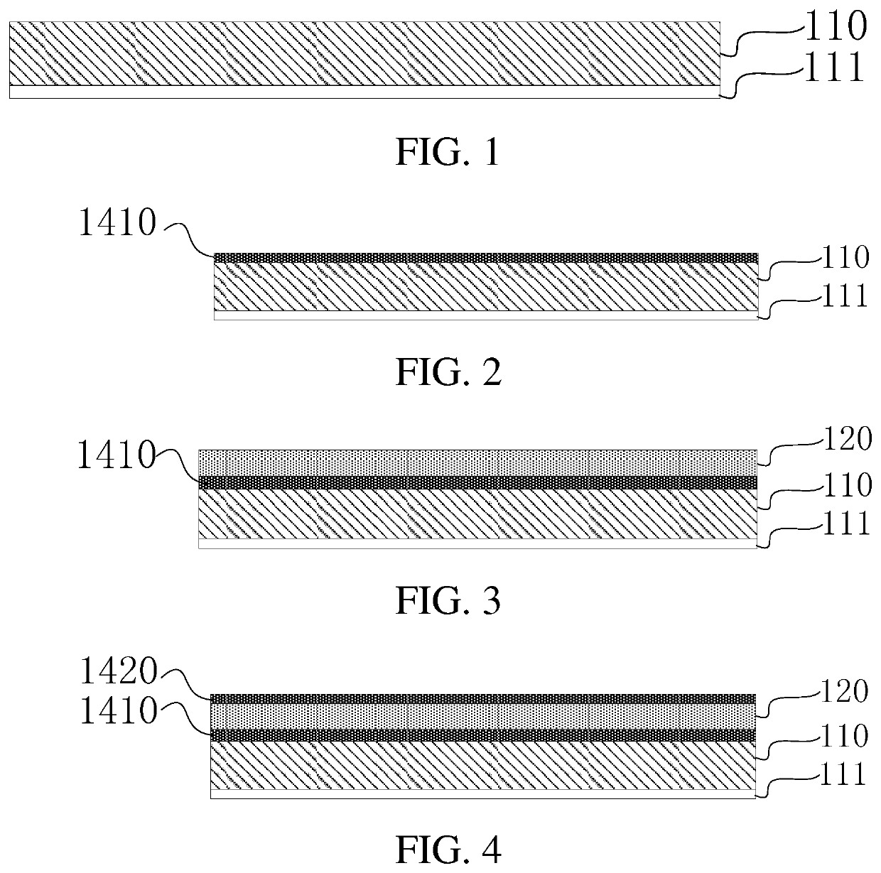
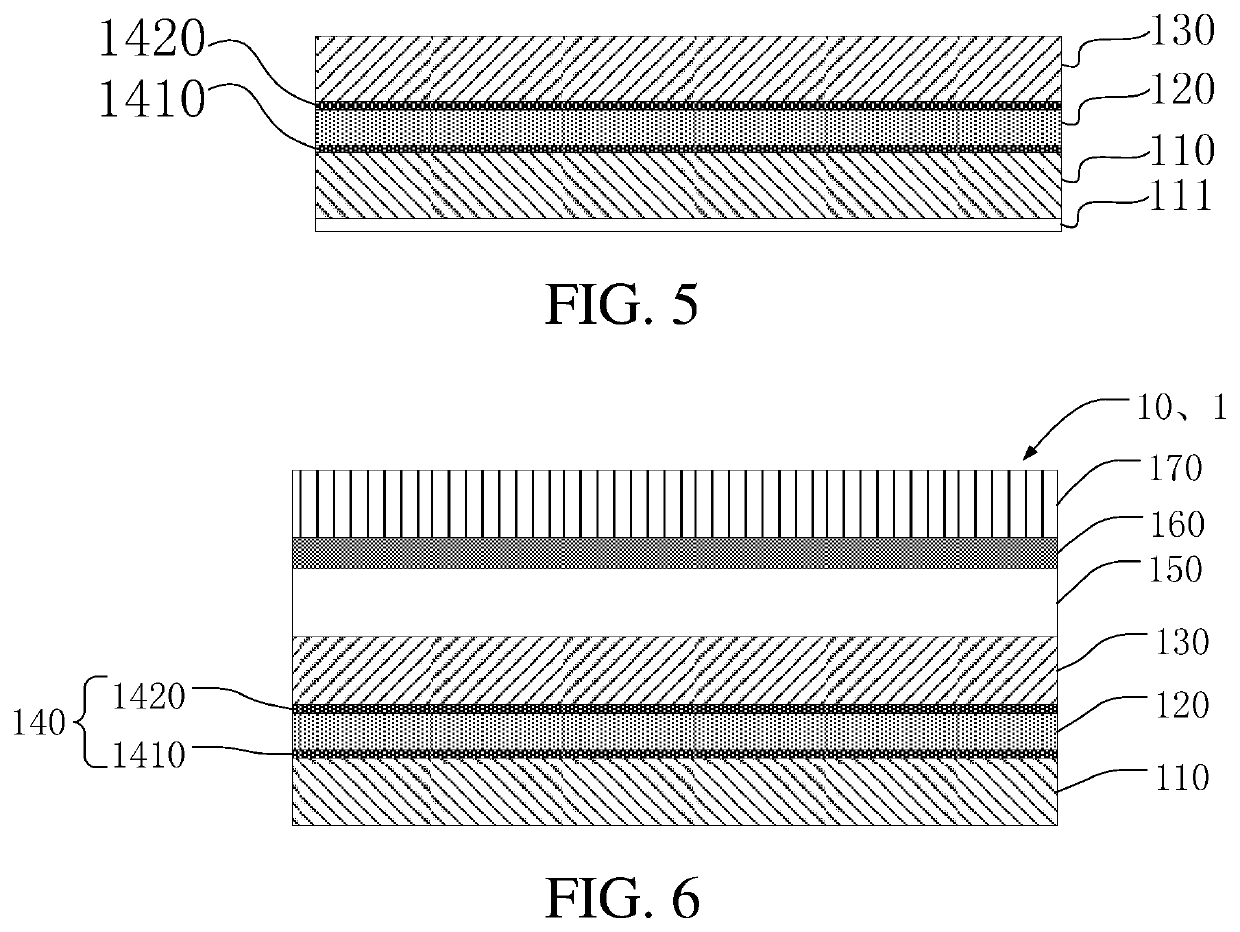
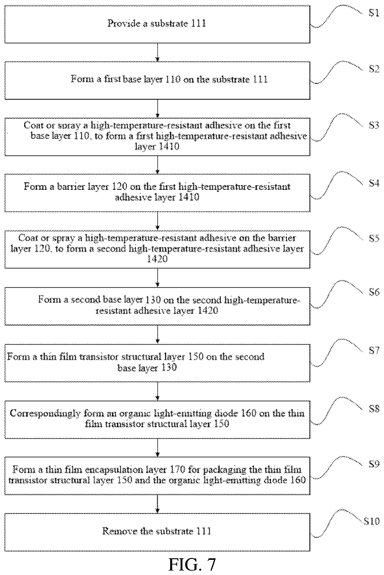
[0034]As shown in FIG. 6, in the present embodiment, a display panel 10 in the present invention includes a first base layer 110, a barrier layer 120, a second base layer 130, high-temperature-resistant adhesive layer 140, a TFT structural layer 150, an OLED 160, and a TFE layer 170.

[0035]Materials used for the first base layer 110 and the second base layer 130 are PI. The barrier layer 120 is disposed between the first base layer 110 and the second base layer 130. The barrier layer 120 may be prepared by a silica (SiO2) material, or may be prepared by a silicon nitride (SiNx) material. Thicknesses of the first base layer 110 and the second base layer 130 are 5 μm to 15 μm. A thickness of the barrier layer 120 is 0.1 μm to 2.0 μm, and specifically, may be 0.2 μm, or 0.5 μm, or 1.1 μm, or 1.9 μm.

[0036]In the present embodiment, the barrier layer may be a single-layer silica layer, or may be a single-layer silicon nitride layer, or certainly, may be a multi-layer structure in which si...


PUM

PropertyMeasurementUnit
temperature-resistantaaaaaaaaaa
thicknessesaaaaaaaaaa

Abstract

A display panel and a preparation method therefor, and a display device are disclosed. The display panel includes a first base layer; a barrier layer, disposed on the first base layer; a second base layer, disposed on the barrier layer; a first high-temperature-resistant adhesive layer, configured to adhere the first base layer to the barrier layer; and a second high-temperature-resistant adhesive layer, configured to adhere the barrier layer to the second base layer. Beneficial effects: An inorganic high-temperature-resistant adhesive layer is coated between the base layer and the barrier layer, so that the base layer can be adhered to the barrier layer more firmly, to improve bending performance of the base layer, and reduce a risk of a fracture between the base layer and the barrier layer, thereby improving a bending capability of the flexible display panel, and improving a product yield, controllability, and endurance.

Description

FIELD OF INVENTION[0001]The present invention relates to the display field, and in particular, to a display panel and a preparation method therefor, and a display device.BACKGROUND OF INVENTION[0002]An organic light-emitting diode (OLED) display panel has such advantages as self-illumination, high contrast, a small thickness, a wide viewing angle, and a high response speed, is the representative of a new-generation plane display technology, and is increasingly praised highly by the industry. A flexible OLED display panel is one of the important development trends.[0003]A flexible OLED display panel is lighter and thinner, and can reduce power consumption, thereby helping improve a battery life of a corresponding product. In addition, because of bendability and flexibility of the flexible OLED display panel, the flexible OLED display panel is also more durable than an ordinary hard display panel. Flexible OLED display panels can be widely applied to products having a display function...

Claims


Application Information

Patent Timeline
Patent Type & Authority Patents(United States)
IPC IPC(8): H01L27/32H01L51/52H01L51/56
CPCH01L27/3244H01L51/56H01L51/5253H01L2227/323H10K59/12H10K77/111H10K59/873Y02E10/549H10K71/80H10K2102/361H10K2102/351H10K2102/311H10K50/844H10K71/00H10K59/1201
Inventor XIA, CHEN
Owner WUHAN CHINA STAR OPTOELECTRONICS SEMICON DISPLAY TECH CO LTD
Features
  • R&D
  • Intellectual Property
  • Life Sciences
  • Materials
  • Tech Scout
  • Unparalleled Data Quality
  • Higher Quality Content
  • 60% Fewer Hallucinations
Learn More