Fixing ESD path resistance errors in circuit design layout

a technology of path resistance and circuit design, applied in the field of electronic design automation, can solve the problems of affecting the profitability of a circuit device, unable to commercially viable development a modern circuit design from concept to physical circuit device, and short circuits in metal interconnects, etc., to achieve fast and efficient compliance, reduce total ground path resistance, and quickly identify

Active Publication Date: 2021-01-05
SYNOPSYS INC
View PDF12 Cites 6 Cited by
  • Summary
  • Abstract
  • Description
  • Claims
  • Application Information

AI Technical Summary

Benefits of technology

The present invention is an improved method for debugging and achieving compliance with ESD ground path rules in a circuit design. The method involves calculating the resistance contribution ratio of each component path structure (polygon) in the non-compliant ESD ground path and identifying the most-problematic polygons with the highest resistance. A report is then generated that prioritizes or emphasizes the most-problematic polygons for corrective action by the user / designer. This method allows designers to efficiently achieve compliance with ESD protection rules using substantially less processing time than conventional approaches. The resistance contribution ratio is calculated by partitioning the ground path model to form a resistor network using its component polygons as edges disposed between corresponding nodes, extracting an associated component parasitic resistance for each polygon, and then determining the total path resistance using the delta voltage values, a source point voltage, and an injected current applied between end nodes of the ground path. The report can be generated using a table-type or graphical-visualization-type report that prioritizes at least one of the most-problematic layer or polygon for corrective action. The ESD correction method can be implemented in an EDA toolset as part of an improved physical verification tool that utilizes an ESD debugging module to verify compliant ESD ground paths and generate reports for non-compliant ESD ground paths.

Problems solved by technology

Moreover, because the post-fabrication discovery of design flaws can cause significant production delays and significantly affect profitability of a circuit device, EDA tools have become essential in the pre-fabrication testing / verification of modern circuit designs.
That is, without EDA software tools, the commercially viable development a modern circuit design from concept to physical circuit device would be practically impossible.
Such an ESD event often produces a high voltage (e.g., several kV) and a high surge current (e.g., 1-10 A) that passes from one input / output (I / O) pad to another I / O pad through the IC's core circuitry, whereby significant heat generated in the circuit structures along the surge current's path (i.e., due to the circuit structures' parasitic resistances) can produce short circuits in metal interconnects and significant damage to the various electrical elements forming the IC's core.
ESD protection can present a special problem to design engineers because all circuit designs must include ESD protection circuits that comply with ESD protection rules established by semiconductor fabrication facilities (i.e., foundries such as TSMC).
That is, many design rules established for a given circuit design are defined by the design engineers, and therefore these design rules may be changed or disregarded when a design engineer finds it difficult to achieve compliance.
Generally speaking, lower path resistances are able to pass higher surge currents without damage than higher path resistances, but all path structures introduce some parasitic resistance, so it is not possible to produce a zero resistance ESD ground path.
Specifically, currently available conventional physical verification tools generate error reports that provide an identifying name / number and non-compliance of each non-compliant ground path (e.g., inform the designer / user that an identified ground path has a 5Ω total path resistance, which exceeds an exemplary 1Ω constraint value by 4Ω), and displays the non-compliant ground path on a layout editor.
Although the conventional ESD verification, analysis and debugging techniques mentioned above were adequate for less complex circuit designs, today's circuit designers are finding it increasingly difficult to efficiently debug non-compliant ESD ground paths in modern circuit designs using only an identify and layout display of each non-compliant ground path.
In contrast, the ESD ground paths used in modern ICs present much more difficult debugging problems due to a substantially larger number of polygons and design layers.
As can be appreciated from the simple example depicted in FIG. 13, the task of debugging even relatively simple few-hundred-polygon ESD ground paths can be difficult when the main source of non-compliance is concentrated in one layer or region of the ESD design.
Using conventional physical verification tools, designers are forced to use best-guess-type approaches to select design layers / polygons for correction (i.e., by widening an interconnect line width or adding more metal vias), whereby the erroneous selection and modification of non-problematic areas of a non-compliant complex ESD ground path network produces little or no progress toward achieving compliance, in turn leading to significant product development cycle (time-to-market) delays.

Method used


Image

  • Fixing ESD path resistance errors in circuit design layout
  • Fixing ESD path resistance errors in circuit design layout
  • Fixing ESD path resistance errors in circuit design layout

Examples


Embodiment Construction

, the citation or identification of any publication does not signify relevance or status as prior art for any of the claimed or described embodiments. Paragraphs for which the text is all italicized signifies text that is common to multiple Synopsys patent specifications.

FIELD OF THE INVENTION

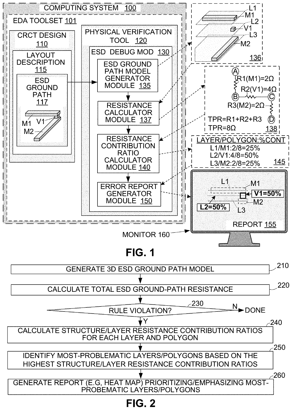
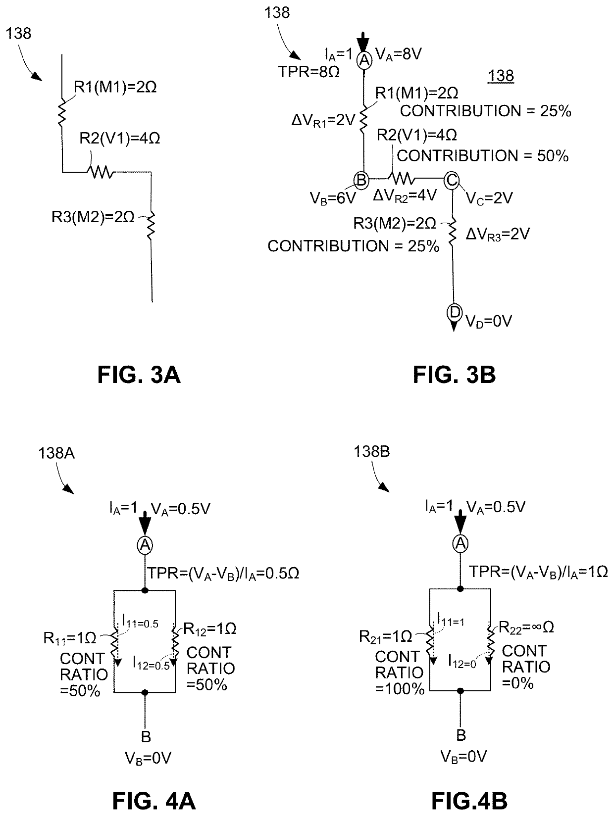
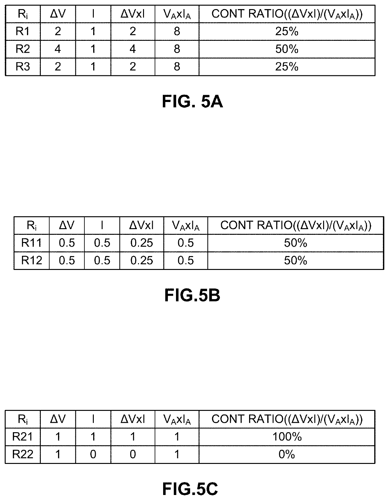
[0004]This invention relates to electronic design automation, more particularly to physical (layout) verification of circuit designs, and even more particularly to physical verification of ESD circuit designs.

BACKGROUND OF THE INVENTION

[0005]Electronic design automation (EDA) toolsets are utilized by circuit developers to design and fully test their circuit designs before manufacturing (i.e., fabricating or otherwise producing) physical circuit structures. The term “circuit design” refers to a software-based description of an integrated circuit (IC) at any stage of the development process, from an initial circuit concept (general system level description) to a final taped-out description suitab...


PUM


Abstract

A physical verification tool for debugging ESD ground path resistance violations in ESD protection circuits. The ESD ground path is modeled and partitioned into component path structures (polygons) that are disposed in associated design layers. A total ESD ground path resistance is then calculated and compared with a maximum allowable resistance value defined by an ESD protection rule. When the ESD ground path is non-compliant, a resistance contribution ratio is determined for each polygon and / or for each layer, for example, by applying nodal analysis to the ESD ground path model. Resistance contribution ratios are then calculated for each polygon and / or for each layer, and most-problematic polygons and / or layers are identified by way of having the highest resistance contribution ratio values. A report (e.g., a table or graphical visualization) is then generated that prioritizes or emphasizes (e.g., by way of a bolder contrast or brighter color) the most-problematic layer and / or polygon.

Description

RELATED APPLICATION[0001]This application claims priority from U.S. Provisional Patent Application 62 / 736,100, entitled “Method for Fixing ESD Path Resistance Error in Chip Design”, which was filed on Sep. 25, 2018, and is incorporated by reference herein.COPYRIGHT NOTICE[0002]The assignee of this patent document has no objection to the facsimile reproduction by anyone of the patent document itself, or of the patent application, as it appears in the files of the United States Patent and Trademark Office, but otherwise reserves all rights whatsoever in any included works of authorship protected by copyright.SPECIFICATION—DISCLAIMER[0003]In the following Background, Summary, and Detailed Description, headings should not be construed as necessarily limiting. In the following Background, Summary and Detailed Description, the citation or identification of any publication does not signify relevance or status as prior art for any of the claimed or described embodiments. Paragraphs for whic...

Claims


Application Information

Patent Timeline
Patent Type & Authority Patents(United States)
IPC IPC(8): G06F17/50G06F30/394G06F30/398G06F111/20G06F119/10
CPCG06F30/394G06F30/398G06F2111/20G06F2119/10
Inventor CHIOU, DE-SHIUAN
Owner SYNOPSYS INC
Why Eureka
Try Eureka