Hermetically sealed isolated OLED pixels

a technology of oled pixels and oled sheets, which is applied in the direction of solid-state devices, semiconductor devices, organic semiconductor devices, etc., can solve the problems of poor moisture barrier properties, inability to use flexible oleds, and brightness non-uniformity, and achieve the effect of improving shelf li

Active Publication Date: 2021-02-02
UNIVERSAL DISPLAY
View PDF90 Cites 2 Cited by
  • Summary
  • Abstract
  • Description
  • Claims
  • Application Information

AI Technical Summary

Benefits of technology

[0013]Some embodiments of the disclosed subject matter disclose a novel thin film encapsulated OLED panel architecture and a method for making the panels with improved shelf life. The OLED panel consists of a plurality of OLED pixels; each OLED pixel is individually hermetically sealed and isolated from its neighboring pixels. More specifically, the organic stack of the OLED pixel is contained within its own hermetically sealed structure. Hermetic sealing is achieved by making the structure on a barrier coated substrate and using a first barrier material as the grid and a second barrier for encapsulating the entire OLED pixel. The first barrier material provides the edge seal while the second barrier disposed over the pixel provides adequate protection from top down moisture diffusion. By isolating and hermetically sealing individual pixels, any damage such as moisture and oxygen ingress due to defects or particles, delamination, cracking etc. can be effectively contained within the pixel thereby protecting the other pixels in the panel. Thus, a long lasting OLED lighting panel can be manufactured.

Problems solved by technology

This traditional encapsulation method makes the display rigid and hence cannot be used for encapsulating flexible OLEDs.
Flexible OLED display and lighting panels fabricated on polymeric substrates such as poly ethylene terephthalate (PET) and poly ethylene naphthalate (PEN), require moisture protection on both the top side and bottom side of the device as the substrates have poor moisture barrier properties.
High sheet resistance of the anode can result in brightness non-uniformity, which becomes more evident when scaling to large-area light panels.
Although, the above (current technology) thin film encapsulated OLED device architectures shown in FIGS. 1-4 have been demonstrated, these panels are not robust against any “damages”.
“Damages” may include defects / particles, pin holes, delamination / cracks induced during flexing or cutting the panel etc.
This would eventually lead to dark spots and a dead panel.
In addition, insulating grids made from polymer materials such as polyimide can be a reservoir of moisture themselves and may damage the OLED devices when the moisture contained within the polymer is released.
Although inorganic grids are effective, it is difficult to process them at low temperatures especially on flexible polymeric substrates.
In most cases, these layers are very brittle and crack when flexed.
Within the OLED device structure, it is well known that the adhesion strength at the organic and cathode interface is weak.
This interface is susceptible to delamination especially when a highly compressive barrier film is deposited over the cathode.
Further, since the organic stack is blanket deposited (continuous), any local delamination / crack occurring at a weak spot in a pixel can propagate across the entire panel, especially after flexing.
Similarly, damages can be induced during the cutting / shaping process of a panel, including: a) electrical short; b) delamination of the cathode and the barrier from the organic (adhesion strength of cathode to organic is very weak); and c) delamination combined with crack propagation when the panel is flexed.
Exposed edges of organic and / or the polymer grid have no protection from moisture leading to a catastrophic failure of the panel.
Delamination or cracks induced by the cutting process tends to propagate across the entire panel; since the weak organic-cathode interface is continuous across the panel leading to a catastrophic failure.

Method used


Image

  • Hermetically sealed isolated OLED pixels
  • Hermetically sealed isolated OLED pixels
  • Hermetically sealed isolated OLED pixels

Examples


embodiment 1

rganic and Cathode Layer, and Blanket Barrier)

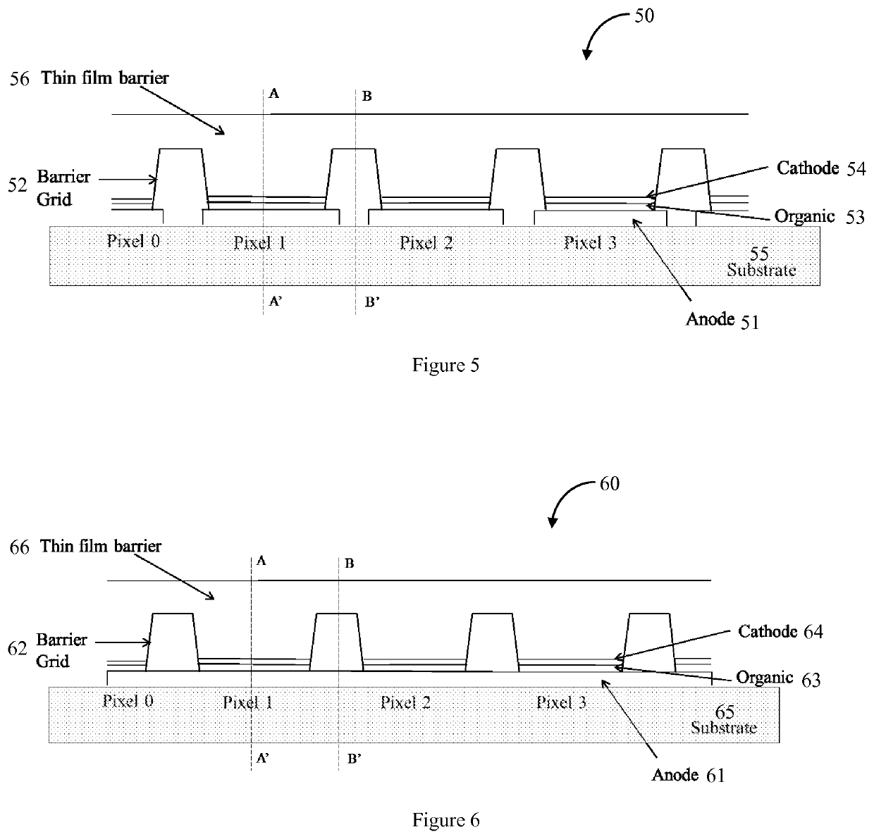
[0047]A cross section of one embodiment of the present invention is shown in FIG. 5. The panel 50 of FIG. 5 consists of a plurality of electrodes (anodes) 51, insulating grid 52, organic stacks 53 and second electrodes (cathodes) 54 between a substrate 55 and a thin film barrier 56. In this figure, a section of the OLED panel containing 3 pixels (Pixels 1, 2, 3) is shown. A lighting panel generally contains a plurality of these hermetically sealed pixels electrically connected to each other. The anode, organic stack and the cathode are patterned. FIG. 6 shows another variation of the current embodiment in which the anode is continuous (not patterned). The panel 60 of FIG. 6 consists of an electrode (anode) 61, insulating grid 62, organic stacks 63 and second electrodes (cathodes) 64 between a substrate 65 and a thin film barrier 66. The grid disposed over a portion of the anode is a barrier material. This barrier grid provides the requir...

embodiment 2

rganic, Cathode and Barrier)

[0054]In another embodiment of the present invention, the top barrier is also patterned to further isolate the pixels. This embodiment is shown in FIG. 11. The panel 110 of FIG. 11 consists of a plurality of electrodes (anodes) 111, insulating grid 112, organic stacks 113 and second electrodes (cathodes) 114 between a substrate 115 and a patterned top barrier 116. FIG. 12 shows another variation of the current embodiment in which the anode is continuous (not patterned). The panel 120 of FIG. 12 consists of an electrode (anode) 121, insulating grid 122, organic stacks 123 and second electrodes (cathodes) 124 between a substrate 125 and a patterned top barrier 126. The organic stacks 123, cathodes 124 and top thin film barrier 126 are patterned. The grid 122 disposed over a portion of the anode 121 is a barrier material. This barrier grid provides the required edge seal for Pixels 1, 2 and 3. The organic stack is patterned in such a way that no organic mate...


PUM

PropertyMeasurementUnit
thicknessaaaaaaaaaa
sheet resistanceaaaaaaaaaa

Abstract

A novel thin film encapsulated OLED panel architecture and a method for making the panels with improved shelf life is disclosed. The OLED panel consists of a plurality of OLED pixels; each OLED pixel is individually hermetically sealed and isolated from its neighboring pixels. The organic stack of the OLED pixel is contained within its own hermetically sealed structure, achieved by making the structure on a barrier coated substrate and using a first barrier material as the grid and a second barrier for encapsulating the entire OLED pixel. The first barrier material provides the edge seal while the second barrier disposed over the pixel provides protection from top down moisture diffusion. By isolating and hermetically sealing individual pixels; any damage such as moisture and oxygen ingress due to defects or particles, delamination, cracking etc. can be effectively contained within the pixel thereby protecting other pixels in the panel.

Description

CROSS-REFERENCE TO RELATED APPLICATIONS[0001]This application claims the benefit under 35 U.S.C. 119(e) of a U.S. provisional patent application of Siddharth Harikrishna Mohan et al., entitled “Hermetically Sealed Isolated OLED Pixels”, Ser. No. 61 / 970,937, filed Mar. 27, 2014, the entire contents of said application being incorporated herein by reference.JOINT RESEARCH[0002]The claimed invention was made by, on behalf of, and / or in connection with one or more of the following parties to a joint university corporation research agreement: Regents of the University of Michigan, Princeton University, The University of Southern California, and the Universal Display Corporation. The agreement was in effect on or before the effective filing date of the claimed invention, and the claimed invention was made as a result of activities undertaken within the scope of the agreement.FIELD OF THE INVENTION[0003]The present invention relates generally to the fabrication of high efficiency OLED devi...

Claims


Application Information

Patent Timeline
Patent Type & Authority Patents(United States)
IPC IPC(8): H01L51/52H01L27/32H01L51/00H01L51/50H01L51/56
CPCH01L51/5246H01L27/326H01L27/3246H01L27/3258H01L51/0097H01L51/5012H01L51/5206H01L51/5221H01L51/5225H01L51/5253H01L51/56H01L51/5209H01L2251/5338Y02E10/549H10K59/122H10K50/813H10K50/822H10K50/844H10K50/8426H10K50/11H10K50/81H10K50/82H10K59/121H10K59/124H10K71/00H10K77/111H10K2102/311
Inventor HARIKRISHNA MOHAN, SIDDHARTHQUINN, WILLIAM E.MA, RUIQINGKRALL, EMORYWALSKI, LUKE
Owner UNIVERSAL DISPLAY
Why Eureka
Try Eureka