
Near-infrared absorbing composition, optical structure, and camera module and electronic device comprising the same

a composition and near-infrared technology, applied in the direction of instruments, group 5/15 element organic compounds, other chemical processes, etc., to achieve the effects of minimizing optical distortion, improving near-infrared absorbance, and low visible absorban

Active Publication Date: 2021-02-23
SAMSUNG ELECTRONICS CO LTD
View PDF30 Cites 0 Cited by
  • Summary
  • Abstract
  • Description
  • Claims
  • Application Information

AI Technical Summary

Benefits of technology

The composition effectively reduces optical distortion by selectively absorbing near-infrared light, enhancing image clarity and maintaining low haze in the visible light wavelength region, thereby improving the reliability and performance of camera modules.

Problems solved by technology

However, when the thin-film optical filter is used to observe and take a picture of a high luminance subject, it may cause a flare phenomenon such as a WiFi-type flare phenomenon that an outline is generated around the subject, a petal flare phenomenon that light is irradiated with the subject as the center, and the like.

Method used


Image

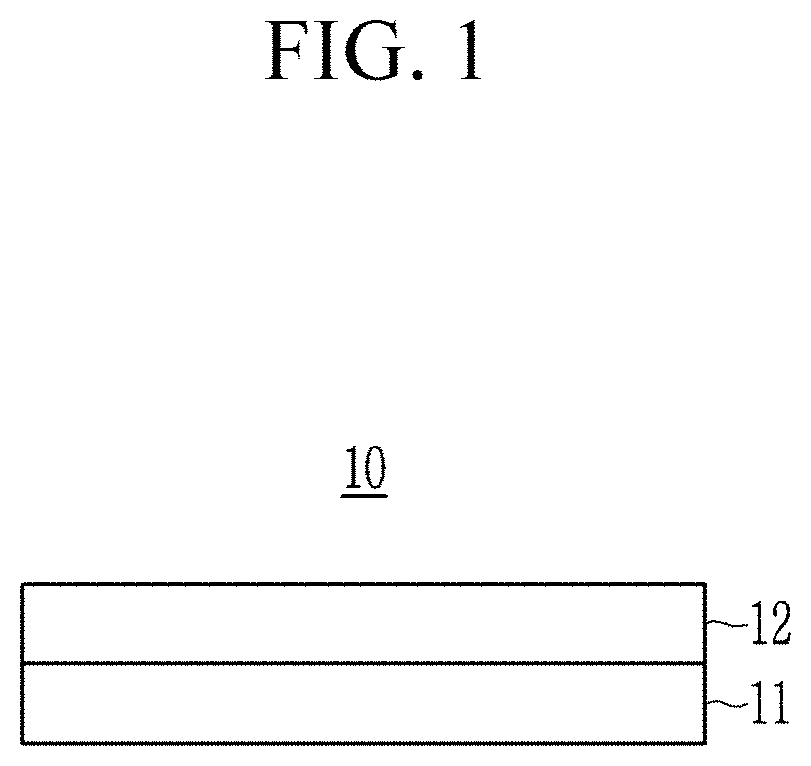
  • Near-infrared absorbing composition, optical structure, and camera module and electronic device comprising the same
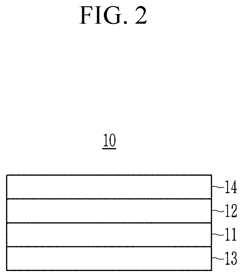
  • Near-infrared absorbing composition, optical structure, and camera module and electronic device comprising the same
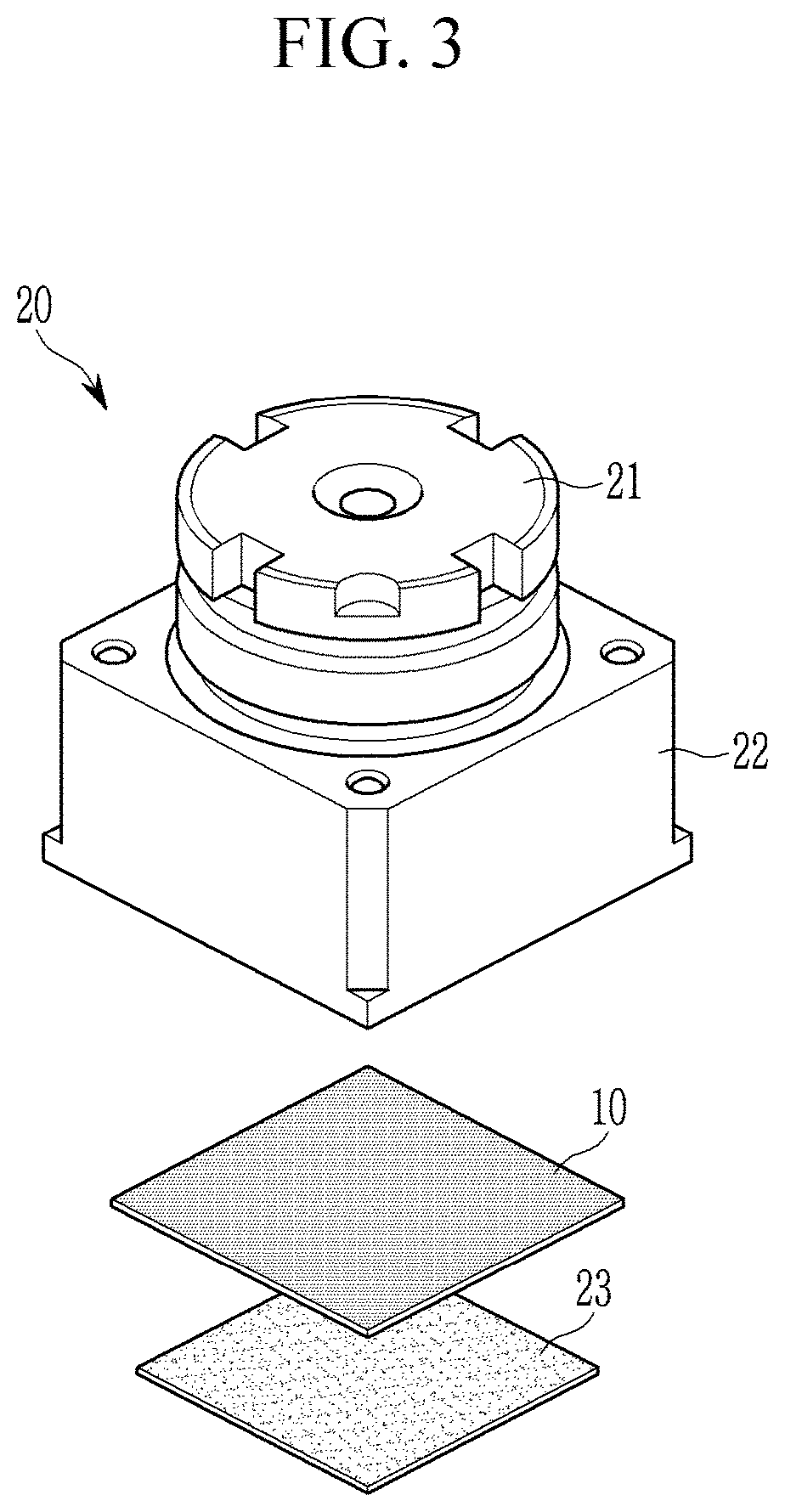
  • Near-infrared absorbing composition, optical structure, and camera module and electronic device comprising the same

Examples


preparation example 1

[0178]10 g of copper (II) acetate (Alfa) is dissolved in a tetrahydrofuran solvent using a magnetic stirrer, 11.57 g of phosphoric acid 2-hydroxy metacryl ester (Sigma-Aldrich) is added thereto, and the mixture is reacted at room temperature for 1 day. 6.06 g of ethyl sulfonic acid (Sigma-Aldrich) is added to the reaction solution, and the mixture is reacted at room temperature for 1 day. Non-reacted particles in the reaction solution are removed through a syringe filter, about ½ of tetrahydrofuran is removed with a rotary evaporator, and a precipitate is obtained therefrom by using hexane, and filtered, and dried at room temperature (10° C. to 30° C.) to 50° C. in a vacuum oven for 12 hours to prepare a copper complex represented by Chemical Formula 1-1.

[0179]

preparation example 2

[0180]A copper complex represented by Chemical Formula 1-2 is prepared according to the same method as Preparation Example 1 except for using 10 g of copper acetate, 11.57 g of phosphoric acid 2-hydroxy metacryl ester (Sigma-Aldrich), and 5.29 g of methane sulfonic acid.

[0181]

preparation example 3

[0182]A copper complex represented by Chemical Formula 1-3 is prepared according to the same method as Preparation Example 1 except for using 10 g, 11.57 g of phosphoric acid 2-hydroxy metacryl ester (Sigma-Aldrich), and 10.47 g of paratoluene sulfonic acid (Daejung Chemicals & Metals Co., Ltd.).

[0183]


PUM

PropertyMeasurementUnit
absorption wavelengthaaaaaaaaaa
cut-off wavelengthaaaaaaaaaa
thicknessaaaaaaaaaa

Abstract

Disclosed are a near-infrared absorbing composition including a copper complex represented by Chemical Formula 1, a near-infrared absorption layer formed by using the near-infrared absorbing composition including the copper complex represented by Chemical Formula 1, an optical structure including the near-infrared absorption layer, and a camera module or an electronic device including the optical structure, wherein Chemical Formula 1 is provided below, andand in Chemical Formula 1, R1, R2, x, and y are the same as described in the detailed description.

Description

CROSS-REFERENCE TO RELATED APPLICATION[0001]This application claims priority to and the benefit of Korean Patent Application No. 10-2018-0087193 filed in the Korean Intellectual Property Office on Jul. 26, 2018, the entire contents of which are incorporated herein by reference.BACKGROUND1. Field[0002]A near-infrared absorbing composition, an optical structure, and a camera module and an electronic device including the same are disclosed.2. Description of the Related Art[0003]Recently, an electronic device including an image sensor that stores an image as an electrical signal, such as a cell phone, a digital camera, a camcorder and a camera, has been widely used.[0004]This electronic device may include an optical filter having a near-infrared absorption capability in order to reduce or prevent generation of an optical distortion by light in the other regions than a visible region.[0005]The optical filter is generally mounted in front of an image sensor of a camera module and thus pla...

Claims


Application Information

Patent Timeline
Patent Type & Authority Patents(United States)
IPC IPC(8): C07F1/00G02B5/22G02B13/00G02B27/10C07F9/09C07C309/04C07C309/30
CPCC07F1/005C07C309/04C07C309/30C07F9/09G02B5/223G02B13/0025G02B27/1013G02B5/208C07F9/091C07F9/12C07F9/11C08K5/521C09K3/00C08K5/36C08K5/005C08J5/18
Inventor KIM, MI JEONGJUNG, MYUNGSUPWON, JONG HOONKIM, CHANGKI
Owner SAMSUNG ELECTRONICS CO LTD
Learn More